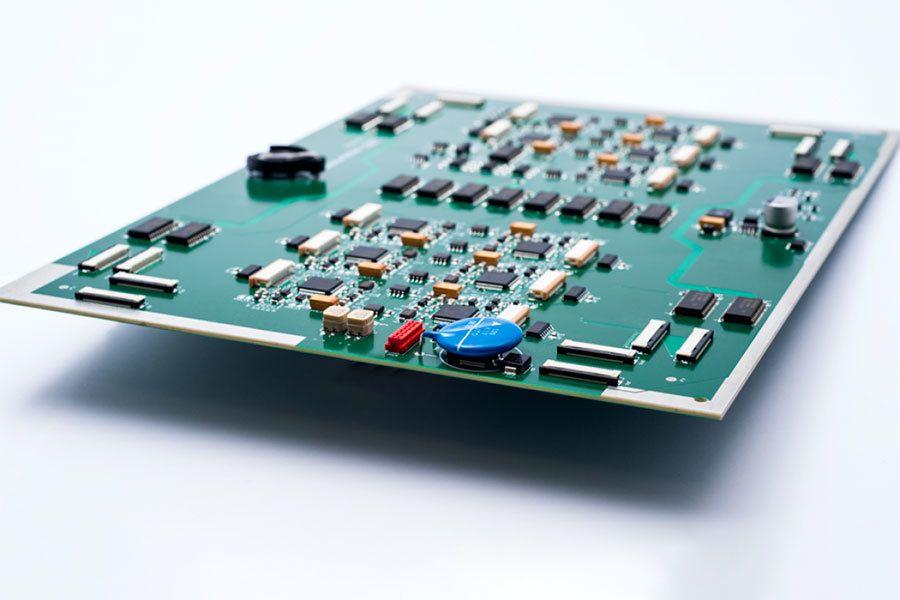
The history of the PCB
Before printed circuit boards appear, the interconnection between electronic components is made up of complete lines by direct connection of wires. Nowadays, a breadboard is only used as an effective experimental tool, and PCB has become an absolutely dominant position in the electronics industry.
In the early twentieth century, in order to simplify the production of electronic machines, reduce the wiring between electronic parts and reduce the cost of production, people began to study the way of printing instead of wiring. Over the past thirty years, engineers have put forward the wiring of metal conductors on insulated substrates. And the most successful is
- In 1925, an American named Charles Ducas printed the circuit pattern on the insulating substrate and succeeded in establishing the conductor for wiring by electroplating. Until 1936, the Austrian Paul Eisler published foil technology in Britain. He used printed circuit boards in a radio device. In Japan, Miyamoto Yoshinosuke successfully applied for special profit by using the spray wiring method (“licensing 119384”). The method of Paul Eisler is the most similar to the printed circuit boards nowadays. This kind of practice is called subtraction, which removes the metal that is not needed. Charles Ducas and Miyamoto Yoshinosuke’s practice is to add only the required wiring, which is called an additive method. Nevertheless, due to the high calorific value of the electronic parts at that time, the substrate of the two parts was difficult to match, so that there was no formal practical application, but also made the printed circuit technology further. In 1941, the United States painted copper paste on talc for wiring.
- In 1943, Americans used technology on military radio.
- In 1947, epoxy resin began to be used as a substrate. At the same time, NBS began to study the manufacturing technology of coil, capacitor, and resistor by using printed circuit technology.
- In 1948, the United States formally approved the invention for commercial purposes. Since the 1950s, the status of vacuum tubes has been replaced by a large number of transistors with low calorific value. Printed circuit technology has been widely adopted. At the time, etched foil technology was the mainstream.
- In 1950, Japan used silver paint as a distribution line on glass substrates, and copper foil on the phenolic substrate (CCL) made of phenolic resin. In 1951, the emergence of polyimide further increased the heat resistance of the resin and made the polyamide substrate.
- In 1953, Motorola developed double-sided plates for electroplating through holes. This method is also applied to the later multilayer circuit boards. 10 years after PCB was widely used, its technology became more and more mature in the 60s. And since the double-faced Motorola, multilayer printed circuit boards have begun to appear, making the ratio of wiring to substrate area more improved.
- In 1960, V. Dahlgreen built a flexible printed circuit board with a printed circuit metal foil attached to thermoplastic plastic.
- In 1961, the Hazeltine Corporation of the United States referred to the electroplating through-hole method and made multilayer boards.
- In 1967, the “Plated-up technology” was published. In 1969, FD-R made soft printed circuit boards with polyimide.
- In 1979, Patel published the “Pactel law” as one of the laws of adding layers.
- In 1984, NTT developed the “Copper Polyimide” method for thin-film loops.
- In 1988, SIEMENS developed Microwiring Substrate’s printed circuit board with an added layer.
- In 1990, IBM developed the Surface Laminar Circuit (SLC) layer printed circuit board.
- In 1995, Panasonic developed an enhanced printed circuit board of ALIVH.
- In 1996, Toshiba developed an enhanced printed circuit board of Bit. In the late 1990s, many printed circuit boards were formally put into practice, until now.


