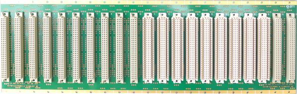
Large Format PCB
 Large Format PCB Manufacturer
 Large Format PCB Manufacturer
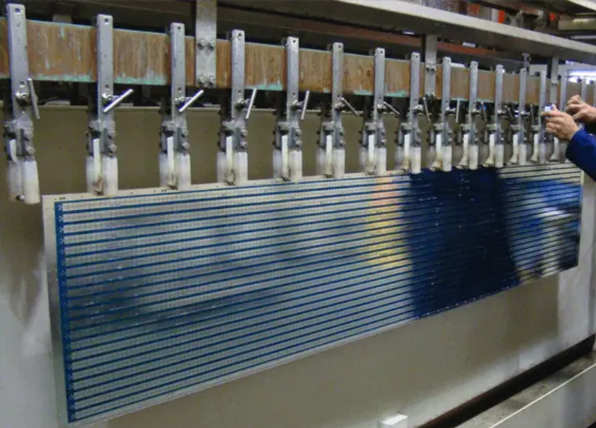
Hemeixin has made substantial investments in the production of Large Format PCB’s. This unique capability allows us to build plated-thru structures up to 24″ wide by 102″ in length utilizing almost any material type.
Hemeixin is one of the few companies in the world who can offer large format PCB for use in RF/Microwave applications. Our continued investment has expanded our capabilities to enable Hemeixin to offer a large range of non-standard PCB. Our auto-clave vacuum oven capability allows Hemeixin to manufacture large format Multilayer PCB.
We produce a variety of large format products every week from Teflon base station antennas to FR-4 lighting structures for commercial airliners. If you require a large PCB let our expert engineering staff assist you. From prototype development to large scale production Hemeixin has the experience and technology to support the most demanding projects. Hemeixin is one of Leading producer for long & large format RF & Microwave PCBs in World!
What is Large Format PCB
irst of all, consider what defines a “large” board: a circuit board that is more than 12 inches wide is large for manufacturing purposes and carries extra requirements. Any layout that is 20 inches long in any dimension would also qualify as a large board. Boards 30 inches wide have reached the limitations of the automated surface mount technology assembly systems. Anything wider will require alternative manufacturing methods, becoming significant cost adders.
The layer count and thickness of the board can also impact the manufacture of a large circuit board. These boards are often used as a backplane, typically requiring many layers. Additionally, these boards usually have many connectors and often include thick power and ground planes. Both of these factors can have an impact on the assembly difficulty.
The largest PCB boards are used industrial settings and communication networks. In addition to holding so many electrical or electronic components, these are PCBs that have to connect to high energy power supplies and cables, and that can be as large as 55” long.
Smaller PCB boards but whose dimensions exceed normal or standard sizes can be found in large electrical equipment and appliances. Although these may not be comparatively large, they present a segment of circuit board sizes that go beyond what considered conventional.
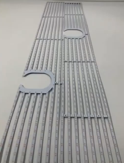
Large Format PCB Technology Capability
- Very Large Format
- Blind and backdrilled thru holes
- Dual diameter holes
- Heavy copper layers
- Connector expertise
- Multilayer structures
- Bonding of large PCB to metal carriers and housing
- Integrated connectors and resistors in RF Feed Networks
| Attribute | Complexity | ||
| Standard | High | Advanced | |
| Layer Count, Maximum | 36 | 60 | >60 |
| Panel Size, Maximum | 21″ x 36″ | 24″ x 42″ | 28″ x 50″ |
| Thickness, Maximum | 0.225″ | 0.400″ | >0.400″ |
| Inner Layer Line Width / Space | .004″/.004″ | .003″/.003″ | <.003″/.003″ |
| Outer Layer Line Width / Space | .005″/.005″ | .004″/.004″ | <.004″/.004″ |
| Impedance Tolerance (SE or Diff) | 10% | 7% | 5% |
| Through Hole Aspect Ratio | 20:1 | 30:1 | >30:1 |
| Drill Registration (no AR). Panel Size Dependent | Drill + 12 | Drill + 11 | Drill + 10 |
| Blind Vias | n to n-1 | n to n-2 | >n to n-2 |
| Buried Vias | No | Yes | Yes |
| Sequential Lamination | No | Yes, < 6 cycles | Yes, > 6 cycles |
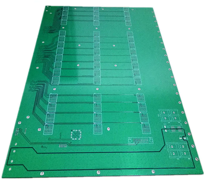
Large PCB Design
If building your large PCB from scratch, the manufacturer will embark on the process to design it. This includes creating the board’s schematics and layout before generating the Gerber files that will be used to fabricate it. The large PCB design process, owing to its unique requirements, requires the designer to ensure the following measures;
- That the board’s signal integrity is taken care of
- That power distribution is optimized, given the many components and board size
- Ensure proper thermal management by incorporating the necessary parts and design requirements for heat dissipation
- That the layering or stack up is designed in a way that allows the board to perform as required, especially when high speed signals are involved
Based on your project needs, the manufacturer will assess your design and advice on various issues such as what can work and what will not work, or the best materials to use, among other things. Some of the materials at your disposal include normal and high Tg Fr4s, aluminum backed substrates for mechanical stability or heat dissipation, and so on.
Considerations to Your Large Circuit Board Manufacturing
High layer count – The higher the layer count is, the more specialized the manufacturer is. This is because many manufacturers tend to offer 2-4, or 6-10 layers. Some do offer 12 or more layers, but they can be very specialized. In addition to this, the more layers you need, the slower the manufacturing process will be.
Quick-turn processes – Not all manufacturers are capable of producing quick-turn PCBs that are large. This is because the amount of copper needed for traces, the high-speed design, and the impedance control can impact the manufacturing process.
The thermal impact – The sheer thickness of the ground planes and their power can have a significant impact on the solder and the soldering process. The more metal that there is on the board, the more solder and heat is required. As a result, it could take a lot longer for the solder reflow profile optimization to be defined.
The price – Typically, when you order more PCBs, the cost of the individual board will be lower. However, if you were to order large printed circuit boards, the cost per board (or unit) won’t be lower. This is because large PCBs do not fit in the panels that are traditionally used when manufacturing boards.
The number of connectors – When many connectors are used on a backplane, much more work is needed to be undertaken to connect the pins and make sure that they work well. This can lead to much longer test times.
All of these factors need to be taken into consideration when a manufacturer is making large printed circuit boards. Please feel free to get in touch with us if you have any questions about the above considerations or anything else. We want you to have large PCBs that work well and do exactly what you need them to do. We’re a friendly team that is here to help.
Large PCB Manufacturing Process
When you ask us to manufacture a large printed circuit board for you, you can trust us to do the job properly. We are here to help you give your customers the best possible PCBs.
Before we agree to manufacture your large PCBs, we will take a look at your design. We want to make sure that every PCB we make is of the highest standard. If we find an issue with your design, we will contact you. We will make you aware of the issue so that it can be corrected.
When this process is complete, we will begin manufacturing your large pcb. Did you know that we check each and every printed circuit board that we make? We want to ensure that you always receive a high-quality PCB from us, no matter how many you have ordered. Whether you order 500 or 5,000 it’s important that every PCB works well for you. If we find a fault in any of the PCBs during our stringent quality checks, we will resolve the issue. We take this step very seriously as we know you’d want us to.
Large Scale Size PCB Prototype Board
At Hemeixin, we’re a team of engineers committed to building electronics for our customers; we have the skills and experience to manufacture boards of all sizes—from small, dense PCBs to large-scale boards with dozens of layers. We have the manufacturing and testing processes and vendor relationships to ensure your large PCB prototype board is built to the highest standards and as quickly and efficiently as possible. Contact us today to learn more about partnering for your next large prototype project.
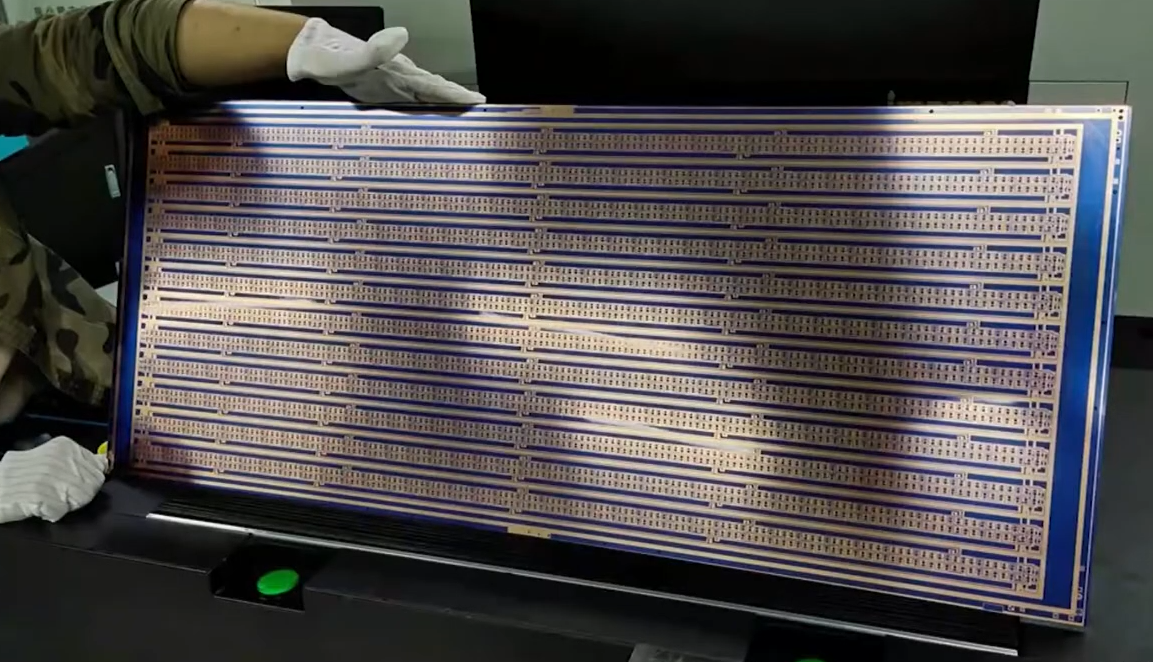
Large PCB Production
After the design and prototyping stages, the manufacturer will produce your large printed circuit board. This requires specialized equipment than what is usually used for standard sizes boards. Generally, the process to fabricate or assemble large format PCB boards is characterized by the following:
Higher Cost: a large board will generally cost more to fabricate. That’s because it uses more materials, in addition to requiring more personnel and other resources such as specialized equipment. The actual price will, however, depend on the design complexity and specific size.
Longer Turn-Around-Time: with its bigger surface area, a large size PCB board takes longer to design and fabricated than regular boards. Your manufacturer can provide you with an estimation of the turn-around time, and these are different across different companies.
Again, the actual TAT will largely depend of the complexity of your project. Also, the number of boards that you want designed and manufactured, among other considerations.
Fabrication and Assembly Challenges: when the PCB is too big, it often may not fit conventional automation assembly methods such as component placement robots or jigs.
In some cases, therefore, the manufacturer may need to install new equipment. Most often, though, large PCB fabricators indicate the maximum sizes that can make. This eliminates the need for changes.


