High Layer Count PCB
 High Layer Count PCBs
 High Layer Count PCBs
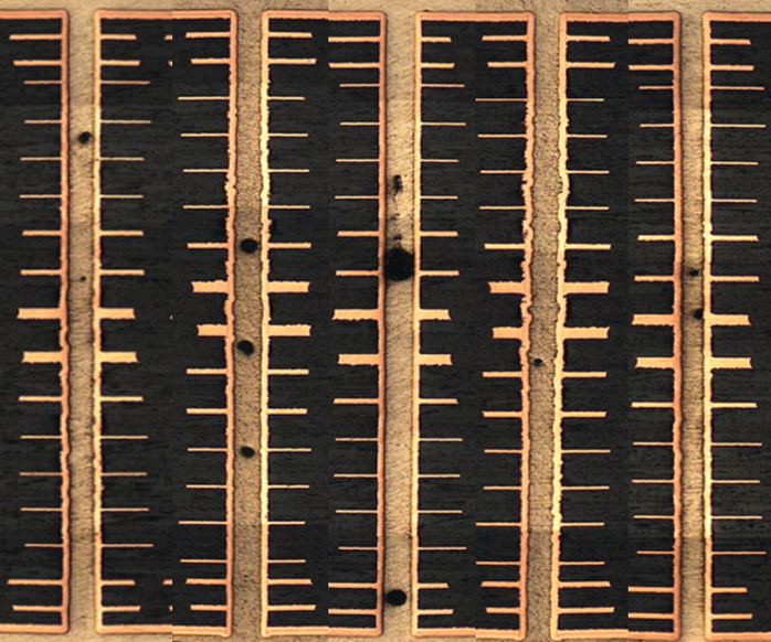
High layer count PCBs, widely found in file servers, data storage, GPS technology, satellite systems, weather analysis and medical equipment are usually ≥12L with special performance requirement raw material.
Taking advantage of our total strength in PCB manufacturing, Hemeixin provides low-cost and high-reliability high layer count PCBs from our domestic and overseas production bases in a timely manner. By supporting the fine pitch with the technology of high alignment accuracy as well as applying multi-stacked HDI technology using laser via and filled plating, Hemeixin realizes the multi-layer substrate structure with the high degree of wiring freedom. In addition, Hemeixin achieves reduction in the number of layers and cost by offers tailored to customers from PCB design to implementation.
High Layer Count PCB Technology Capability
- Reliability test system that meets the requirements of the major global server providers;
- Meet major global server equipment providers’ requirements for signal loss measurement and verification
- Master the expansion and contraction control technology of various materials
- Rich experience in using low-loss materials
- Have a dedicated FAE team for technology and design that cooperates with customer in product development.
High Layer Count PCB Applications
- Communication base station network devices
- High-speed and large-capacity optical fiber devices
- Communication devices
- Measurement devices
- Computer peripherals
- Medical devices
High Reliability High Layer Count PCB
Data centers, communications systems, and high-performance computing require thick boards with dense circuitry to accommodate today’s advanced high bandwidth applications. Compared to previous generations of technologies, these electronics house boards are even thicker and have longer operating lifetimes than in previous generations. Our high-performance through hole electroplating processes enable printed circuit board (PCB) manufacturers to reliably connect the layers of thick multilayer boards with excellent microdistribution and minimal surface copper plating.
Our High Layer Count PCB features
Our High Layer Count PCB manufacturing process benefits from the following features:
- Press platens are heated by means of circulated “hot-oil”, ensuring no localised hot-spots in the bonding process and minimising the risk of bow and warpage.
- Lamination under vacuum eliminates air-entrapment
- X-ray drilled PTH holes ensuring optimum registration of drilled holes to copper lands
- Welded “inner-layer” books to eliminate lateral movement of inner layers during the press cycle and to maintain optimum registration of inner layers
- Digital printing of inner layer pairs with integrated side-to-side line-up to printed tooling targets ensuring optimum registration

- Automatic optical inspection
- 100% electrical test
- Test coupons and micro-sections
- Non-destructive plating copper thickness measurement
All copper, solder resist and component ident layers are printed digitally (without photography) with line up machine controlled to fiducial markers, achieving exceptional registration standards.
We develop copper through hole plating solutions that bring upgraded technology for a range of board sizes, so that no matter what kind of high layer multilayer board you are manufacturing, it can be built with more reliability and with less surface copper than before.


