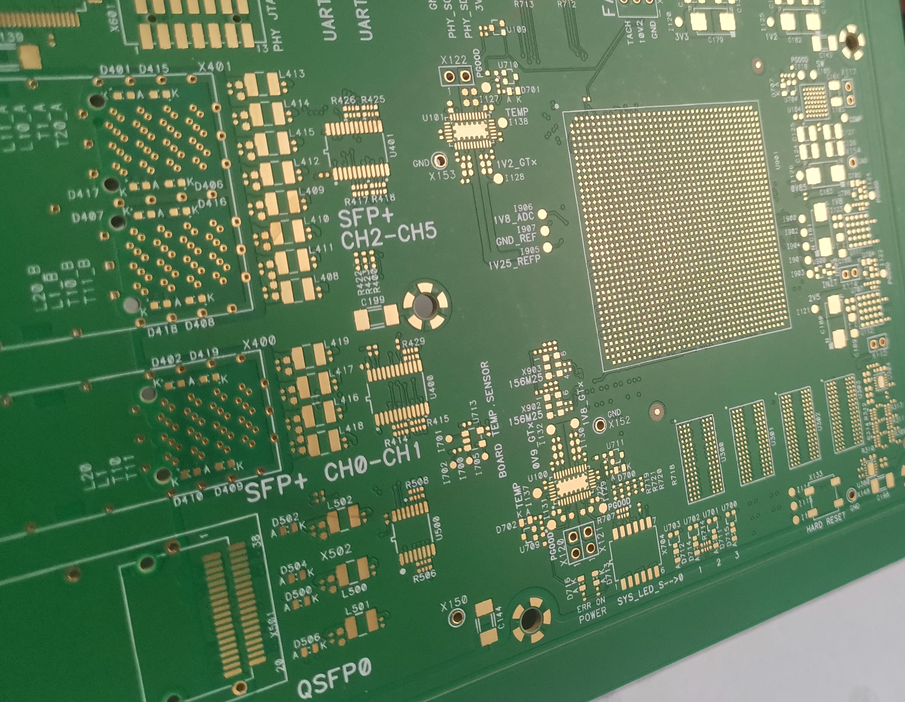
What is an ELIC HDI PCB?-Any layer HDI PCB
The popularity of HDI and HYBRID PCB has increased considerably over the years, mainly as a result of manufacturing innovation. This type of PCB is used in high-end electronic, industrial, and military applications where a great deal of I/O is needed, often with more than one layer. For example, an Electronic Layer Interconnect Circuit board, or ELIC for short, is a type of high-density interconnects printed circuit board. The goal was to reduce the size of boards while improving performance and reliability. They were designed to be used with other devices in a high-density harness and fit in smaller places than traditional PCBs. For example, they are found in weapon systems on surface ships, aircraft, and submarines due to these devices' space restrictions.
In this guide, we will look at the benefits and applications of an ELIC PCB and an introduction to what makes this unique, alternative PCB technology tick.
What is ELIC HDI PCB: An Overview
ELIC HDI PCB is a new high-density interconnect technology that offers a small form factor and low profile. It is the first time ELIC technology has been used on a PCB.
ELIC HDI PCBs are manufactured using a proprietary technology that allows the traces to be formed on all layers of the board simultaneously. This means that instead of having to drill holes through the board and solder wires to them, you can run your signal through the board itself, at any point in its thickness, without any degradation in signal integrity.
ELIC traces do not require impedance matching because they are self-impedance matched at each end. This means they can be routed in any direction, regardless of trace length or impedance requirement. The only constraint is reliability: because circuits are shorter than traditional designs, there is less copper available for each signal trace, so there may be a limit on how many signals can be routed per layer before reliability becomes an issue.
As with conventional HDI PCBs, ELIC HDI PCBs use blind and buried via technology to connect all the substrate layers. The critical difference is that ELIC HDIs use an extra layer of copper between each pair of ground planes to create pathways for vias that pass through all three dimensions. These pathways form a grid over the board's entire surface area, enabling more vias per square inch than conventional HDI PCBs. The result is more copper traces, and copper fills per square inch than traditional one-dimensional PCBs.
Characteristics and Advantages of ELIC HDI PCB
Smaller Size
HDI PCBs allow you to fit more components into a smaller area, allowing you to create smaller devices that consume less power than their larger counterparts. This also makes them ideal for creating wearable electronics such as smartwatches and other wearables.
Flexible Mounting Options
ELIC HDI PCB can be bent around corners without breaking or cracking because of its flexible nature and lack of an external coating like conformal coatings (CC). This makes it ideal for use in tight spaces where bending around corners would otherwise be impossible with traditional rigid PCBs.
Faster Speed
Because ELIC HDI PCBs are so small, they can operate at higher clock speeds than traditional solutions, resulting in faster processing and data transfer rates. If you are designing a device that needs to process large amounts of data quickly or transmit large files over long distances quickly (such as with cellular communications), this is one of the essential advantages of ELIC HDI PCBs over other options such as FPGA chipsets or discrete components.
Excellent Heat Dissipation Performance
Due to the use of copper foil as substrate material, which has excellent thermal conductivity, ELIC HDI PCB can dissipate heat quickly with less thermal stress generated during operation. Therefore, this type of board performs well in high-temperature applications such as circuits for industrial robots and semiconductor manufacturing equipment. It can also be used in low-temperature environments without affecting its performance.
Short Lead Time
Because the production process is relatively simple and no complex processes are involved in making this type of circuit board, its production cycle is shorter than other circuit boards such as FR-4 boards and glass fiber boards.
High Reliability
ELIC HDI PCBs have a strong anti-jamming capability and are more reliable than traditional printed circuit boards because, besides withstanding high temperatures, they also withstand humidity, static electricity, and electromagnetic interference (EMI). This makes them ideal for performing well in harsh environments such as oil fields, chemical plants, power plants, and military equipment applications.
Applications of ELIC HDI PCB
The ELIC HDI PCB board is an excellent fit for many applications, including:
Medical Devices: The ELIC HDI PCB can be used in the medical field, such as ultrasound imaging equipment, blood analyzers, etc.
Electronic Components: The ELIC HDI PCB can be used for electronic components such as power supplies, audio amplifiers, etc.
Audio Equipment: The ELIC HDI PCB can be used for audio equipment such as speakers and headphones.
Automobile Electronics: The ELIC HDI PCB can be used for automobile electronics such as car navigation and infotainment systems.
Final Thoughts
An ELIC HDI PCB is a very specific piece of electronic hardware, and while they exist, they are not very common. At first glance, it looks like a traditional printed circuit board. But the ELIC HDI is far more than what meets the eye, as it includes some unique features which have made it popular among designers and inventors alike who want to create a circuit board that can be mass-produced at low cost. If you want to use this type of PCB in your next product, contact HemeixinPCB. Hemeixin manufactures high-quality PCBs that are a perfect fit for your needs.


