How to BGA Fanout Routing in your HDI PCB
HDI stands for High-Density Interconnect. As the name suggests, an HDI PCB is characterized by its high density of components and routing interconnections that use the latest PCB technologies. An HDI design is by its very nature a high-performance design.
HDI design uses the latest advances in the PCB interconnection technology. Keeping in mind the latest state of the art PCB technology, we can define the HDI PCBs as those printed circuit boards that use some or all of these features: microvias, blind and buried via/microvia techniques, built-up PCB laminations and high-signal performance considerations.
What is an HDI PCB Layout?
High density interconnect (HDI) layout refers to a set of techniques used to layout a PCB when traces widths generally drop below 8 mils (0.2 mm). These techniques are designed to ensure you can fit a higher density of components onto a single board, allowing you to keep your board size small while increasing component count. Not all boards need HDI PCB layout techniques for a number of reasons, while some components require HDI techniques for proper routing.
An HDI PCB board requires smaller vias to make layer transitions, particularly in fine-pitch BGA components and more traces per sq. mm. In order to accommodate fine-pitch components, you'll find the following typical features in an HDI PCB layout:
- Smaller vias: HDI boards use microvias (mechanically or laser drilled), blind/buried, and staggered vias for layer transitions. These vias have smaller aspect ratios than typical through-hole vias. In order to use these vias with finer pitch components, their diameters are smaller, which then limits their useful depth.
- Thinner traces: The thinner traces used in HDI PCB boards are required to make connections to vias on each layer, as well as to in-pad vias. The thinner traces also allow higher trace density, thus the term HDI.
- Higher layer count: We've built non-HDI boards with high layer counts, but HDI board layer counts can easily reach 20 or more layers when working with high pin density components (e.g., FPGAs).
- Lower signal levels: HDI boards are not used for high voltage or high current. This is because the high field strength between neighboring lines will cause ESD, and high currents will cause excessive temperature rise in conductors.
If you look at the above points and the IPC standards, you can figure out when a board makes the transition to the HDI regime, thus requiring HDI PCB layout and routing techniques. According to the IPC-2221A/IPC-2222 standards, the maximum recommended aspect ratio for through-hole vias is 8:1 (aspect ratio = via depth/via diameter). This means, for a standard thickness 1.57 mm PCB, the minimum drill diameter for a through-hole via is 0.196 mm, or ~8 mils. If your vias need to be smaller to accommodate fine-pitch components, then you'll need to use some HDI-specific via designs and thinner traces.
Trace Sizes and Vias in Your HDI PCB Layout
Clearly, the need accommodate fine pitch components or simply a higher density of components is what motivates the need for HDI pcb designs. Traces are fabricated in the same manner as traces on any other PCB, although care is taken to prevent over-etching. Vias are a different beast and may require laser drilling (for low aspect ratios) through a single layer, known as blind or buried vias.
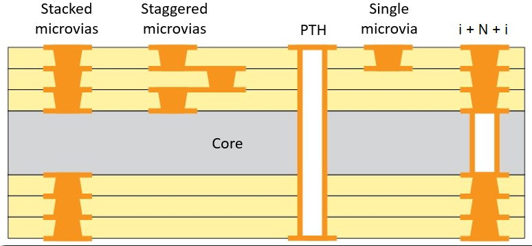
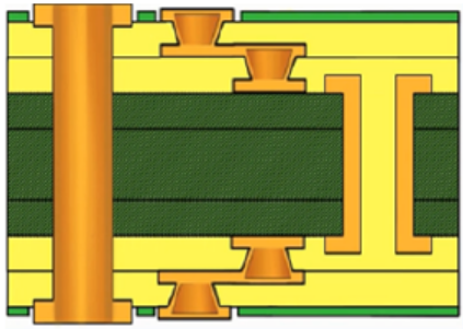
If you need to span multiple layers in an HDI board, you can't use a through-hole via anymore and still comply with IPC standards. For larger diameter microvias, some manufacturers has experience fabricating blind vias that span multiple layers, but this is not common. Furthermore, placing this in your design will likely violate your manufacturer's DFM rules and will cause your board to receive no-bid status. Instead, vias can be placed in individual layers and stacked on top of each other (e.g., stacked microvias or blind-buried vias). The various microvia configurations are shown below.
These different via configurations are primarily targeted at BGA components with different pitch. Once your BGA pitch gets to 0.8 mm, you'll likely be able to use a dog bone fanout with in-pad microvias. At 0.75 mm and less, you're better off using plated in-pad microvias (VIPPO) to reach inner signal layers, although you can also route signals between BGA pads to reach the outer pad section during fanout. At much lower pitch (e.g., 0.5 mm), it is not recommended to route between pads unless your manufacturer can reliably fabricate traces below 4 mils.
Basic HDI PCB Design Guidelines
When working with fine-pitch BGA, and the traces and vias that connect to it, there are some basic guidelines that apply to any HDI layout.
- Always check your manufacturer's capabilities. You should generally do this anyways before planning a new design, but nowhere else is this more important than in HDI design. Not all manufacturers have the same capabilities in this area, and it's best to check with your desired manufacturer before you create an HDI layout that can't be fabricated.
- Keep track of spacing between traces and pads. The same idea applies in 1 mm pitch BGAs, the only point that changes is scaling to microvia sizes. Solder mask clearance values are typically on the same size as your trace width. The solder mask clearance depends on the pad size and your pad pitch.
- Don't use staggered vias or ELIC if you don't need them. The whole point of HDI routing is to provide as much space as possible for routing on the surface and inner layers. While it might be tempting to stack across the entire span of the substrate, don't take up the extra space unless it's really necessary.
- Opt for fewer layers. High layer count boards bring more assembly steps and manufacturing costs. If you follow the previous guideline, you can significantly reduce the cost per board.
- Don't forget about signal integrity when working with HDI boards. Any HDI layout will need to be designed with high speed design guidelines in mind, or high frequency guidelines if you're working with an RF PCB board. The same signal integrity rules that apply in typical PCBs still apply in HDI PCBs, it's just a matter of scaling. In an HDI board that requires impedance controlled routing, you'll need to carefully design your traces and stackup to ensure your impedance is consistent with your signaling standard.
See also: HDI PCB design guidelines
Overview of HDI PCB Board Design and Manufacturing Processes
There are a number of steps involved in the typical PCB manufacturing process, but HDI PCB manufacturing uses some particular steps that may not used in other boards. The HDI board design process starts like many other processes, where the
- Determine the layer count required to route all signals, either by using the largest BGA component on the board or by using the interface + direction count from the largest IC on the board.
- Contact your fabrication house to select materials and obtain dielectric data to create your PCB stackup.
- Based on layer count and thickness, determine the via style that will be used to route signals through inner layers.
- Perform a reliability assessment if relevant, to verify that the materials will not stress interconnects to fracture during pcb assembly processing and operation.
- Determine design rules based on fabricator capabilities and reliability requirements (need for tear drops, trace widths, clearances, etc.) to ensure reliable manufacturing and assembly.
Stackup creation and determination of design rules are the critical points as they will determine ability to route the board and reliability of the end product. Once these points are completed, a designer can implement their fabricators DFM requirements and reliability requirements as design rules in their ECAD software. Doing this on the front-end is very important and it will help ensure the design is reliable, routable, and manufacturable.
The Key to HDI PCB Design Success
As a designer, the first step in the HDI design workflow is to determine whether or not you need HDI. You should have an idea by looking at your schematic and your target board. HDI PCB layer stacks are also can ask common options provided by Hemeixin HDI PCB fabrication house.
Once you determine that you require HDI, you need to look at the stack-up. Don’t use more than three sequential layers unless there is absolutely no other solution. We recommend that you use a good fanout strategy for complex ICs, like BGAs and QFNs – this will help you reduce the number of sequential laminations if you plan your fanout strategy properly.
Choose the right HDI PCB material
Material selection is, of course, important for all PCB designs. It is especially important for HDI PCB manufacturing because there are additional manufacturing constraints that play a role. The goal is always to select the right material for manufacturability that, at the same time, meets your temperature, and your electrical requirements. Also, make sure that your high-speed material is also suitable for your HDI design. They are many other factors that come into play when selecting the proper materials for your design.
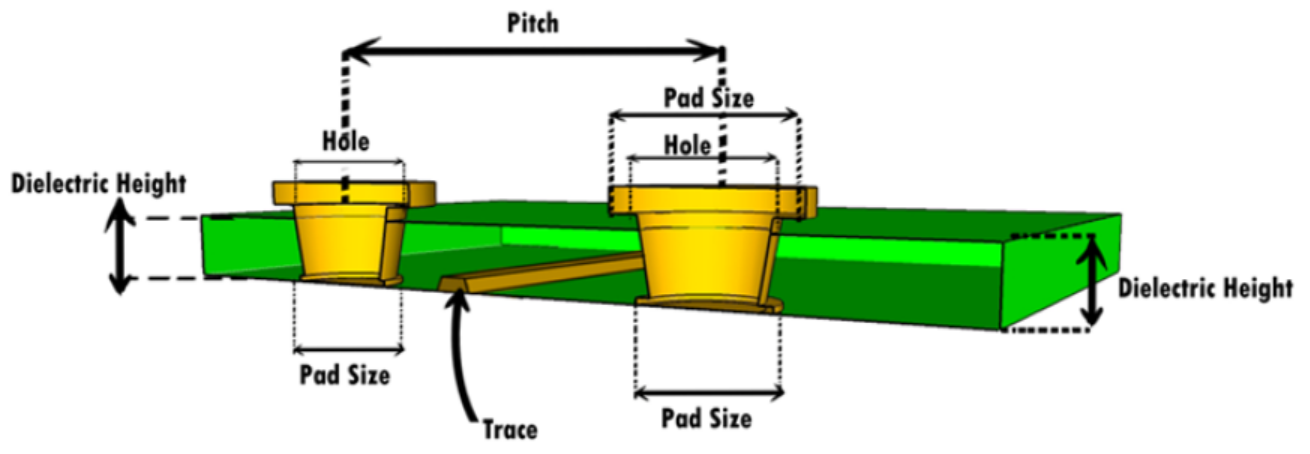
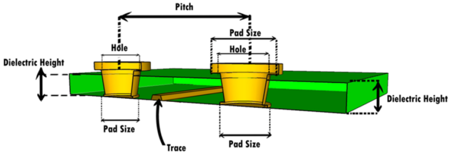
Proper material selection is important for the layout design since materials will affect the electrical performance of the signal traces. The physical thickness of the material is important when considering the aspect ratio of the microvia to be plated. The current standard aspect ratio for a microvia is 0.75:1. (The microvia diameter should be larger than the height of the material it is penetrating to the next adjacent layer.)
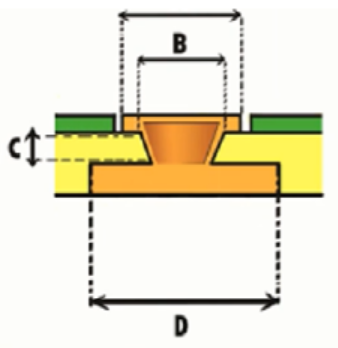
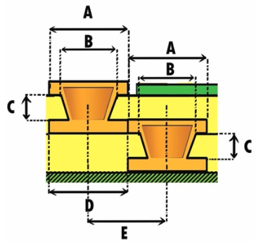
ASPECT RATIO OF LASER-DRILL MICROVIAS
- RATIO OF LASER MICROVIA = C/B:1
- MOST PRODUCTIVE AND COST-EFFECTIVE A/R IS .75:1 OR LESS
|
Microvia Hole Diameter |
Maximum Dielectric Layer Thickness(mils) |
|||
|
A/R=0.5 |
A/R=0.75 |
A/R=0.9 |
A/R=1 |
|
|
6.00 |
3.0 |
4.50 |
5.40 |
6.00 |
|
5.00 |
2.5 |
3.75 |
4.50 |
5.00 |
|
4.00 |
2.0 |
3.00 |
3.60 |
4.00 |
|
3.00 |
1.5 |
2.25 |
2.70 |
3.00 |
|
2.00 |
1.0 |
1.50 |
1.80 |
2.00 |
Other material considerations are the maximum withstanding temperature, maximum frequency of signals and coefficients of thermal expansion (CTE). The maximum temperature here refers to that temperature which the PCB is required to withstand without affecting its mechanical integrity. It is usually expressed in degrees Celsius. The maximum frequency refers to the highest frequency that the electrical signals realized on the PCB are operating at. This is usually expressed in MHz or GHz. Our engineering staff will ask you the fastest rise/fall time during the circuit operation and help narrow down the selection of materials that would meet your requirements. Along with these items, the dielectric constant of the material and the dielectric loss, or dissipation factor, will also play vital roles in material selection.
If you choose a high-speed material, make sure it is suitable for sequential laminations. When using high-speed materials like Rogers 3000, it is difficult to go through more than one lamination, it is very hard to predict the material movement and make the material really bond well. The material Hemeixin recommends for high-speed HDI is Megtron, Isola I-speed, etc.
When you are designing your stack-up for HDI, know where your cores are and know which ones are your prepreg layers so when you are doing your controlled impedance structure you have an idea of what the possible variation could be in the layer thickness – the distance of the dielectric from the signal layer to the reference plane. There is no harm in using sequential laminations as long as you understand the variations that could happen. If you pick the right material with less glass weave and more resin, you can have more predictability during press-out, which means better predictability in your impedance.
How to plan your pcb stack-up and microvia structure
The microvia structure affects the number of lamination cycles and therefore impacts the manufacturing process and cost.
In conventional multilayer boards, your design choices depend on the number of signal layers you require. HDI offers a larger variety of design choices. Choose from blind and buried, sequential build-up, or stacked and staggered, as well as many other design choices. Of course, HDI does not require complex architectures. One of the most common mistakes designers make is creating architectures that are unnecessarily complex.
HDI stack-up classes
There are different stack-up classes for HDI boards. The first option is a single lamination built using laser drills. This stack-up class is a no-brainer in terms of utilizing microvias in the least expensive way possible: Using only one lamination. When you use a laser drill, you benefit from a smaller pad and via size. This can help ease some of the design restrictions and reduce your design time.
Going over the possible structures, it is important to know the process steps associated with the stack-up. Additional process steps mean more cost and more yield loss.
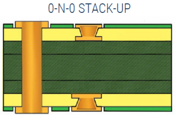
N represents the number of layers in the first or base lamination (or core lamination) and 0 tells that there is no sequential lamination steps and no extra dielectric and copper layers are added.
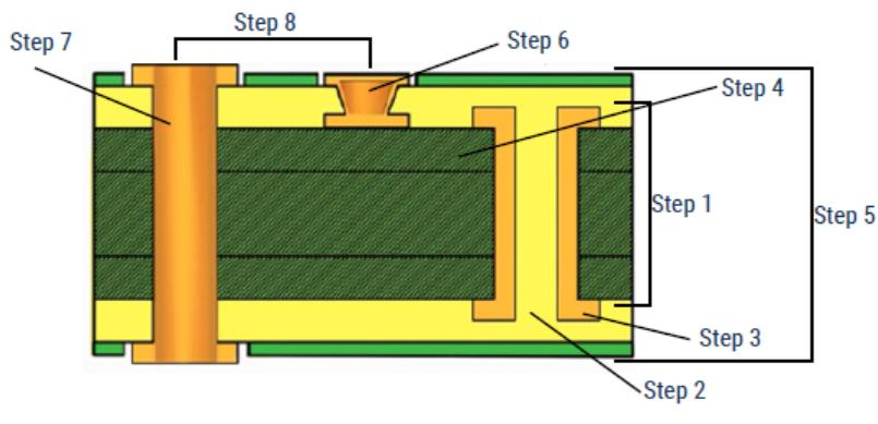
In this 1-N-1 type of stack-up, the ‘1’ represents one sequential lamination on either side of the core. One sequential lamination adds two copper layers for a total of N+2 layers. This stack-up does not feature stacked vias. There is one extra lamination and no stacking of the vias. The buried via has been mechanically-drilled. There is no need to use a conductive fill for the via. It will naturally fill with the dielectric material. The second lamination adds the top and bottom layers.
Then, we finish up with a final mechanical drill. The pcb manufacturer plans the right amount of prepreg between layer one and two so the resin flows into the buried via.
1-N-1 WITH LASER MICROVIAS AND MECANICAL BURIED CORE VIA
Consider whether you need a final mechanical drill. You can get the same connections with the laser drill and the buried mechanical. This saves an extra drill cycle and saves the manufacturer from dealing with the registration of the mechanical drill and the laser drill.
Building this next stack-up takes an additional two laminations for a total of three laminations:
2-N-2 WITH STAGGERED MICROVIAS AND BURIED CORE VIA
The HDI PCB manufacturing steps are as follows:
|
1-N-1 |
2-N-2 |
|
1. The core is laminated. (The core can be only two layers, so no lamination.) |
1. The core is laminated. (The core can be only two layers, so no lamination.) |
|
2. The core is mechanically drilled. |
2. The core is mechanically drilled. |
|
3. The laser drilled vias are formed. |
3. The laser drilled vias are formed. |
|
4. The mechanical drill is plated. |
4. The mechanical drill is plated. |
|
5. Layer two is imaged/etched. |
5. Layer two is imaged/etched. |
|
6. The sequential lamination adds two additional layers. |
6. The sequential lamination adds two additional layers. (The mechanical drill is now a buried via.) |
|
7. (The mechanical drill is now a buried via.) |
7. The laser drilled vias are formed. |
|
8. The laser drilled vias are formed. |
8. Lamination of another 2 layers. |
|
9. The final through-hole via is formed. |
9. Laser drill. |
|
10. The laser drill and the through-holes are plated. |
10. Plating the laser drill. |
|
11. Image and etch. |
|
|
12. Back to lamination. |
The manufacturer will be going back to the laser drill and plating process twice for the laser drills, once for the buried mechanical drill, and then a second time for the through-hole mechanical drills. Each lamination cycle can be done in one day. So with three laminations, this can only be done in three days. Plus an additional day for outer layer processing. Four days in total.
Here are some additional types of stack-ups:
- 0-N-0 with laser microvias
In this stack-up, the manufacturing steps are as follows:
- The core is laminated.
- The core is mechanically drilled.
- The laser drilled vias are formed.
- 1-N-1 with microvia stacked on top of buried and filled core via
This stack-up is similar to the one above, except in this case there are also laser microvias stacked on top of buried core vias. This requires that the buried core vias should be filled and plated before adding the additional two layers. And the microvias need to be plated with copper and planarized flat.
- 2-N-2 with stacked microvias and buried core via
In a 2-N-2 stack-up, the ‘2’ represents two sequential laminations.
As stated above, one sequential lamination adds two copper layers, so two sequential laminations add four copper layers for a total of N+4 layers. Again, there are no stacked vias.
A more complicated structure is called a 3-N-3. At this point, material selection becomes critical. Is your material robust enough to handle four lamination cycles, plus a reflow cycle in assembly, plus a possible rework that you might have afterwards? Let‘s now talk about the cost.
|
Single lamination |
$ |
|
2 SUB construction laminations |
$$ |
|
Staggered vias sequential lamination up to 3 build-up layers |
$$$ |
|
Stacked vias sequential lamination up to 3 build-up layers |
$$$$ |
On the left of this chart, you have HDI PCB stack-up classes, and on the right, you have the associated cost. The more sequential laminations, the higher the cost. The most expensive stack-up class is three sequential laminations. This includes microvias stacked on top of each other, which is necessary when you are breaking out of a tight pitch BGA, like .3 mm. Second in the stack-up class in terms of cost are using a non-conductive hole through process.
When you are placing your vias, you need to know where they are going what layer are they starting from and what layer are they stopping at? Knowing where your drilled holes are is the key to keeping your cost down. Think about the number of times the board has to go through mechanical and laser drill versus just going to laser drill. Most designers think they need mechanical drilling for the power of the pins of the BGA but this is not necessarily true. You do not want an HDI design where right at the center of the BGA there is a through-hole. A through-hole has to align with the laser drilled vias, which makes it harder to manufacture, you might have a lower yield, and you are just adding an extra through-hole process, which you probably did not need at first. The manufacturer has to align mechanical versus laser drilled holes.
Stacked vs staggered vias
Staggered vias essentially mean less process steps. The manufacturer does not have to fill the laser-drilled vias with copper because the second laser drill does not land on the first laser drill. Filling or plating a microvia shut usually happens in a special plating tank designed with chemistry that plates the laser-drilled microvia from the bottom of the via to the top of the via, until the hole is completely filled. Plating a laser-drilled microvia shut adds time and cost to the process and is only needed when you are stacking on an inner layer or if you have a via-in-pad on the outer layer. If the second laser-drilled via is staggered or offset, there is no need to copper plate shut. If you are staggering your laser-drilled microvias, it is important to know what spacing your manufacturer requires between the laser drills.
STAGGERED VS. STACKED MICROVIAS
STAGGERED
-NO COPPER FILL REQUIRED
-NO EXTRA IMAGING STEP
STACKED
-HOLE FILL REQUIRED
-PLANARIZATION REQUIRED
-EXTRA IMAGING STEP
What is the laser drill accuracy? It is very safe to assume it is +/- 1 mil accuracy. Usually, in a staggered microvia formation, the diameters of both operate and lower microvias are the same. The key parameter that decides whether the staggering is possible or not, without the lower microvia needing to be filled, is the dimension E, the vertical separation between the central access of the two microvias. For staggering to be viable, the value of E must be greater than the microvia diameter.
Sometimes, the space restrictions are so tight that your only option is a stacked via. Here are some precautions for stacked vias: Stacking on a buried mechanical drill is known to be a bad structure where failure can occur. We have seen cracks at this connection. We have not seen cracks on stacked laser-drilled microvias.
The final point is: If you have a buried via, it is better to offset your laser drills from the buried mechanical drills and then stack from that point onwards. This gives you the most reliable connection.
Key considerations in your HDI PCB design strategy – a checklist
Via diameter, pad diameter, trace width and space, and aspect ratio.
Take into account a complete view of the design before deciding the via and pad sizes you are implementing, so you don't paint yourself into a corner. The primary consideration at this point in the planning stage is routing density. Routing density is determined by the high-pin count fine pitch device on the board, for example, a BGA. BGA pin count and BGA pitch are both important parameters that affect routing density.
When you are deciding your BGA pad size, do take into account the assembly process and the PCB design rules that you are following. For example, pad to pad spacing and soldermask web are two critical design parameters. If you are choosing a via-in-pad approach, your BGA pad size needs to account for the size of the laser and mechanically drilled microvias while keeping the correct pad size required by the BGA assembly process.
The BGA pad size and the microvia size should be determined along with the trace width and spacing. Depending on the pitch of your BGA (say for example, 0.8 mm), the trace width and the via sizes will determine an optimum number of signal layers. At Hemeixin, we have created an HDI Design Planning Tool (with requisite algorithms) that assists our engineering staff in specifying an optimum via size, pad size, and trace width depending upon the desired number of signal layers.
You can see what an important role via sizes, pad sizes, and trace width and space play in the overall stack-up structure.
When you design an HDI PCB board, make sure that you have your aspect ratios right for the plating process. To achieve acceptable copper plating, the plating solutions have to properly fill the hole. If the hole sizes are too small compared with the thickness of the PCB, you might get unsatisfactory plating.
See also: HDI PCB design guidelines
The constraints of controlled impedance
Controlled impedance for HDI has some additional issues. HDI has thinner dielectrics than traditional boards, so if you are looking for a traditional 50-ohm single-ended or 100-ohm differential pair, the thinner dielectrics will require less wide traces. That is why it is possible to have a higher density of interconnections in an HDI PCB board. You can design with 5-mil trace and space, but it is a lot better if you are using 3.5-mil trace and space, as that matches the 3 or 4-mil dielectrics on the buildup. As such, it is important that the fabricator knows how to control the tolerance of a 3.5 or 3-mil trace, in order to meet that characteristic impedance.
In order to get a higher impedance, you must have:
- Thinner traces
- Thicker dielectrics
- Less copper
- Lower dielectric constant (Dk)
- More space in between differential pairs
In order to get a lower impedance, you must have:
- Thicker traces
- Less dielectrics
- More copper
- Higher dielectric constant (Dk)
- Less space in between differential pairs
When you are trying to design appropriated trace widths for controlled impedance lines, it is important that you use the correct thicknesses for the dielectrics between the signal layers and the reference planes. The dielectric thickness to be taken is what is called the press-out thickness.
Another challenge in HDI PCB technology is that you have to use the correct thickness of the copper layers in the built-up layers resulting from sequential lamination. Pay attention or things could go wrong.
The base thickness of the material is found on the material data sheets or is available from the laminate manufacturers. PCB manufacturers calculate the final press-out thicknesses that they expect from the prepreg, which depends on the amount of resin in the prepreg, the amount of the copper area percentage, and the thickness of the adjoining copper layers. PCB manufacturers calculate the copper area percentage from the CAD files that you sent. Therefore, they do not follow the generic thickness specified on the data sheets, they use the calculated press-out thicknesses for impedance modeling, which will change from design to design. This will require small adjustments in the trace widths and spacing of the controlled impedance traces. If Hemeixin cannot meet the impedance requirement that you are looking for with the dielectric thicknesses or material types you have selected, Hemeixin will suggest an alternative dielectric thickness or PCB material.
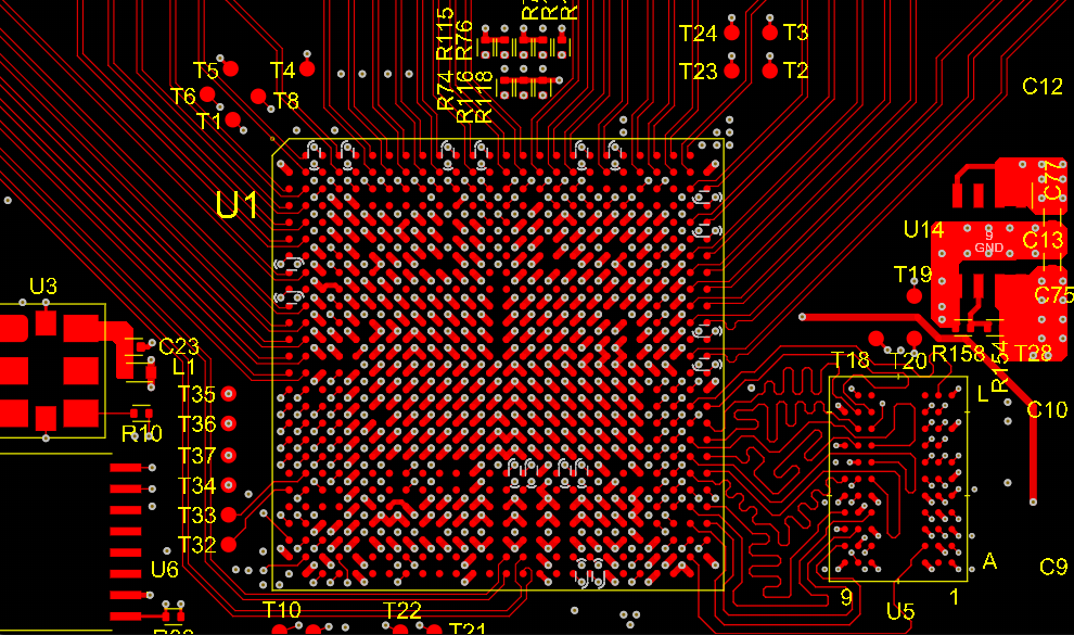
HDI PCB BGA breakout and fanout strategy
BGAs have the highest density of I/O connections and array pins on a device, which is the most complex part of the layout.
BGA breakout means applying a fanout solution and routing traces from those fanouts to the perimeter of the device prior to general routing of the PCB.
“Be careful about drawing the connections all at once. It is a good design practice to do the layout part by part. If you have a BGA, the first goal is to go out of the BGA. Be sure that you can go out with all the pads and all the pins under the BGA. Do not fully route all the interfaces, but instead just route a little bit of track, and then stop routing to place vias, or draw the tracks for different parts just a little bit out of the BGA area. Make sure that you will be able to fanout and connect all the pads under the BGA. You can then start connecting all the interfaces.
If you only draw short tracks, it is very easy to delete them and redo parts of the layout under the BGA because you did not fully route the tracks. So you can just delete them and try to find a way to fanout all the pins. This practice is much easier and will save you a lot of time since you only have to deal with a small part of your layout. You want to avoid finding yourself in a difficult position once you have fully routed your BGA and you need to take out only one pin, for example. If that happened, you would have to deal with a lot of tracks just to be able to remove one signal.
There are some exceptions, like memories or high-speed interfaces. In this case, you can fully route the connections between the BGA and the memories or the high-speed interfaces before you finish the fanout of all the pads.”
Example of how to breakout a .4mm BGA
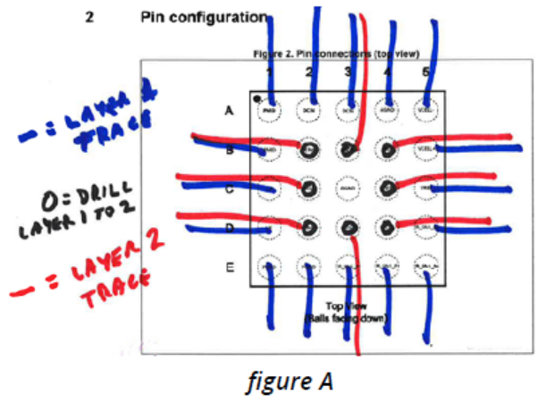
When planning out how to breakout (or route) a .4mm BGA, the overall size and the pin out of the part need to be thought through so the most cost efficient technology can be used. It is not just about the fact that the pads are .4mm apart and figuring out what are the numbers of widths and gaps that work. When fanning out a .4mm BGA, the geometry does not work out so that you can route a trace between the pins. The traces and gaps are just too small to go down enough layers to get all the pins fanned out. So with a .4mm BGA, blind and buried vias are required. The pins on the outside row in the BGA are routed on Layer 1, the pins on the next row in the BGA are routed on Layer 2 etc. The way the BGA is pinned out will determine how to route the BGA.
In this configuration above, the problem is what can you do with the GND pin? Drilling from Layer 2 to Layer 3 will cost more.
Example of how to route a .4mm BGA:
This part is a standard .4mm BGA. The best way to fan it out is to use blind and buried vias and a multi-lamination fabrication.
Start off by adding a Layer 1 to Layer 2 blind via on all of the GND pins of the BGA. (This is a hole in the BGA pad that will tie that pin to the GND plane on Layer 2.) Now all of the GND pins are done and do not need to follow the routing described below.
The routing plan:
Route the outside row or ring of pins (24 pins, row 1 and 7 and A and G) on the top side of the board, Layer 1. You may need to route out some of the GND pins on the outside row and not just add a 1 to 2 via in the BGA pad.
Add a Layer 1 to Layer 2 blind via to the next ring of pins (16 pins, row 2 and 6 and B and F), route this ring out on board Layer 2 – Layer 2 is a GND plane so these Layer 2 routes can only route out a short distance and then a standard top to bottom via is added. Do not cut off the GND plane with these short Layer 2 routes such that the GND plane is cut up and pins are not connected.
Then, on the next ring of pins (8 pins, row 3 and 5 and C and E), add a Layer 1 to Layer 2 blind via and a Layer 2 to Layer 3 buried via and route these nets out on board Layer 3.
Pad and drill sizes for .4mm BGA:
There will be no traces between pads on the top layer so the pads can be 10 mils and have a 5.7 gap between them. For the larger pad, let the manufacturer drill a 4 to 6-mil laser drill for the buried and blind vias. The distance between the board layers will determine the best drill size so they can plate the hole shut and make a flat pad for the BGA, etc.
Sequential lamination:
Let's pretend that this is an 8-layer board.
Board Layers 2 through 7 will be laminated together. Then, a laser drill will be done from Layer 2 down to Layer 3: This is your 2 to 3 buried via. Note that a Layer 7 to 6 buried via could also be used, and a Layer 2 to 7 could be used; but the 2 to 7 needs to have bigger drill and pad.
|
BGA Area Microvia 0.4 mm Pitch |
||
|
Drill Size |
Pad Size |
Trace |
|
4 mils |
6.75 mils |
3 mils |
Board Layers 1 and 8 will now be laminated to the board and a laser drill will be done from Layer 1 down to Layer 2 (Layer 10 to 9 if needed).
Then, the standard through via is drilled top to bottom – here again, bigger drill and pad are required.
In your Gerber files, you have parts placed around the .4mm BGA. The fanning out and adding standard size vias and trace width and spacing will take up a lot of room around the BGA.
Technology level for .4:
|
For BGA Pitch - 0.4 |
TECH I |
TECH II |
|
BGA area MicroVia Drill/Pad Dia in mils |
6/12 |
4/6.75 |
|
BGA area BAse Core Via Drill/Pad Dia in mils |
6/12 |
6/12 |
|
BGA Area Trace width and spacing Top Layer |
5 |
5 |
|
BGA Area Trace width and spacing inner Buildup Layers |
5 |
3 |
|
BGA Area Trace width and spacing inner Core Layers |
5 |
5 |
|
BGA Area Trace width and spacing Bottom Layer |
5 |
5 |
|
# of Traces bet BGA pads on : Top layer |
0 |
0 |
|
# of Traces bet BGA vias on: Inner Buildup Layers |
0 |
1 |
|
# of Traces bet BGA vias on : Inner Core Layers |
0 |
0 |
|
# of Traces bet BGA vias on: Bottom Layer |
0 |
0 |
Example of how to breakout a .5mm BGA:
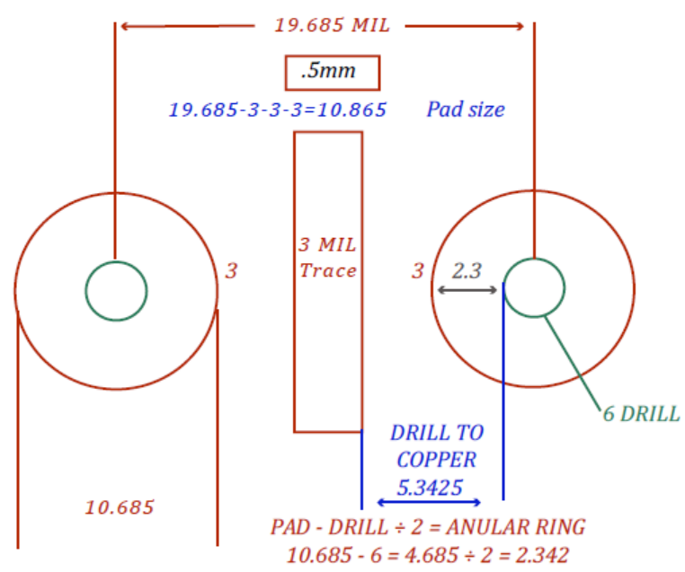
This example is from a board with pitch at .5mm (19.685 mils) and the minimum drill size is 6 mils. The minimum trace width needs to be 3 mils and the trace to pad spacing also needs to be 3 mils.
Take the BGA pitch minus the 3-mil trace minus the 3-mil trace to pad gap minus another 3-mil trace to pad gap and you have a pad diameter (or a pad size) of 10.685 mils. 19.685 – 3 – 3 – 3 = 10.685
Now take the pad size of 10.685 mils minus the 6-mil drill size divided by two and you have a 2.3425-mil annular ring on the pads. 10.685 – 6 / 2 = 2.3425
On a plane layer:
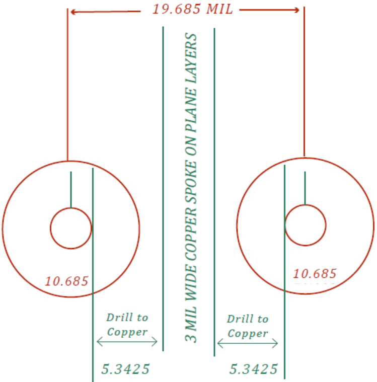
If the via ties to the plane, it will be a solid tie (no thermal relief). If the via does not tie to the plane or to a signal trace on this layer, the pad on this layer can be removed. You can set up your design software to suppress unconnected pads and it will remove the pads on non-functional pins.
On a .5mm BGA, the copper spoke between the drills will be 3 mils wide. The distance from the edge of the drill to the edge of the 3-mil copper spoke between the drills is the drill-to-copper spacing. With the above sizes, the drill-to-copper will be 5.3425 mils. The drill-to-copper spacing required to manufacture the PCB changes due to many different factors. There is no set rule of thumb size for all boards.
This works if the board is 62 mils or less thick and does not have more than eight layers. The board thickness and the layer count have an increase in accumulative tolerances, which explains why fewer layers on a thinner board helps a lot.
Set up the footprint of the part with the via-in-pad– ie. a drill in the surface mount component pad of the BGA. The manufacturer might adjust the trace and space a little but can build the board with these numbers.
|
BGA Area Microvia 0.5 mm Pitch |
||
|
Drill Size |
Pad Size |
Trace |
|
6 mils |
10 mils |
3 mils |
Technology level for .5:
|
For BGA Pitch - 0.50mm |
TECH I |
TECH II |
TECH III |
|
BGA area MicroVia Drill/Pad Dia in mils |
6/12 |
6/10 |
5/9 |
|
BGA area BAse Core Via Drill/Pad Dia in mils |
8/14 |
7/14 |
6/12 |
|
BGA Area Trace width and spacing Top Layer |
5 |
5 |
5 |
|
BGA Area Trace width and spacing inner Buildup Layers |
5 |
3 |
3.5 |
|
BGA Area Trace width and spacing inner Core Layers |
5 |
5 |
5 |
|
BGA Area Trace width and spacing Bottom Layer |
5 |
5 |
3.5 |
|
# of Traces bet BGA pads on : Top layer |
0 |
0 |
0 |
|
# of Traces bet BGA vias on: Inner Buildup Layers |
0 |
1 |
1 |
|
# of Traces bet BGA vias on : Inner Core Layers |
0 |
0 |
0 |
See also: HDI PCB design guidelines
Just as Moore's Law has brought transistor gate sizes to ever smaller dimensions, PCBs have followed suit. Although HDI layout is not a new technique, it is critical in many systems that have high component count and high net count. These boards have enabled many new products, such as new smartphones, powerful custom computers (such as those we build for our customers), networking equipment, and much more.
Designers don't normally plan to create an HDI PCB layout unless they are working with specific components that require such layout and routing techniques. On the contrary, they are often forced to work in the HDI regime for a number of reasons. If you suspect you'll need to work with component densities that require HDI layout and routing, here's what you need to know about your next board and how to plan your design.
HDI PCBs have high-density attributes, including laser microvias, sequential lamination structures, fine lines, and high-performance thin materials. This increased density enables more functions per unit area. Advanced technology HDI PCBs have multiple layers of copper-filled stacked microvias, which creates a structure that allows even more complex interconnections. These complex structures provide the necessary routing and signal integrity solutions for today's large pin-count, fine pitch, and high-speed chips in high technology products.
