- Home
- PCB Prototype
- Assembly
- PCB
- Rigid-Flex PCB
- Technology
- PCB Material
- Epoxy Filled Vias
- Heavy copper circuit board
- HDI Micro vias PCB
- Controlled Impedance
- RF & Microwave PCB
- Rigid-Flex Circuit
- Bending And Folding
- Thermally Conductive PCB
- Flex PCB Design Guidelines
- Rigid-flex PCB design guidelines
- HDI PCB design guidelines
- Heavy copper PCB design guidelines
- Flexible PCB design issues
- Flex-Rigid PCB design issues
- Turn-key PCB Assembly design issues
- PCB Trace Width Calculator
- Company
- Quote

-
Epoxy Filled Vias
Via In Pad PCB
Hemeixin offers a variety of printed circuit board manufacturing solutions for Plug Via Process requirements. Whether you require vias flooded with mask, selective plugging in BGA areas, conductive and non-conductive epoxy fill, or fully plugged and via in pad, we have you covered.
In HDI PCB design, via refers to a pad with a plated hole that connects copper tracks from one layer of the board to other layer(s). High-density multi-layer PCBs may have blind vias, which are visible only on one surface, or buried vias, which are visible on neither, normally referred to as micro vias. The advent and extensive use of finer pitch devices and requirements for smaller size PCBs creates new challenges. An exciting solution to these challenges uses a recent, but common PCB manufacturing technology with self descriptive name, “via in pad”.
Filled via in pad is a way to achieve intermediate density with an intermediate cost compared to using blind/buried vias. Some of the key advantages associated with using the via in pad technology are:

- Fan out fine pitch (less than .75mm) BGAs
- Meets closely packed placement requirements
- Better thermal management
- Overcomes high speed design issues and constraints
Filled and capped vias
Filled and capped vias: At first, a non-conductive/conductive medium is filled and is left for hardening. Next, the ends are planarized and metalized. Then these are plated over to make the surface solderable. This is the technology in via-in-pads. These types of vias help in saving space.
IPC-4761 specifies 7 different types of vias:
Tended (Via Type I-a/-b) and Tented and covered (Via type II-a/-b) A via with a dry film mask material applied bridging over the via wherein no additional materials are in the hole. Via type II is Via type I with an additional cover. Prior to surface finish. Type II is not supported anymore
Plugged (Via Type III-a/-b) A via or through hole with material applied allowing partial penetration into the via or through hole. The plug material may be applied from either one or both sides of the via structure. (Prior to surface finish.)
Plugging and covered (Via Type IV-a/-b) : A via or through hole with a secondary covering of mask material applied over the plugged via. The material may be applied from either one or both sides of the via structure. (Prior to surface finish.)
Filled (Via Type V) : A via or through hole with material applied into the via or through hole targeting a full penetration and encapsulation of the hole. (Prior to surface finish.)
Filled and covered (Via Type VI) : A via or through hole with a secondary covering of material applied over the filled via or through hole. The material may be applied from either one or both sides of the via structure. (Prior to surface finish.)
Filled and capped (Via Type VII) : A via or through hole with a secondary metallized coating covering the via or through hole. The material may be applied from either one or both sides of the via structure. (Prior to surface finish.)
| Type | Description | Covering-Material |
| I-a / -b | Tented one-sided / double-sided | Dryfilm solder-stop |
| II-a / -b | Tented & Covered one-sided / double-sided | Dryfilm solder-stop + LPI solder-stop |
| III-a / -b | Plugged one-sided / double-sided | Plugging Epoxy (non-conducting paste) |
| IV-a / -b | Plugged & Covered one-sided / double-sided | Plugging Epoxy + LPI solder-stop |
| V | Filled | Plugging Epoxy (non-conducting paste) |
| VI-a / -b | Filled & Covered one-sided / double-sided | Plugging Epoxy + LPI solder-stop |
| VII | Filled & Capped | Special Plugging Epoxy + plating |
i.e. low inductance
- No via plugging is required at component locations
- Provides a flat, coplanar surface for component attachment
Via Fill Options
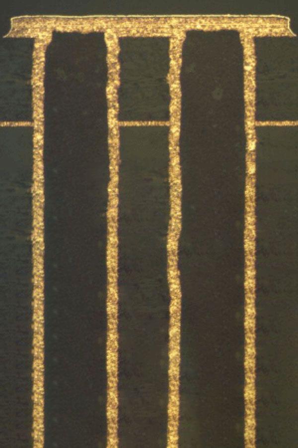
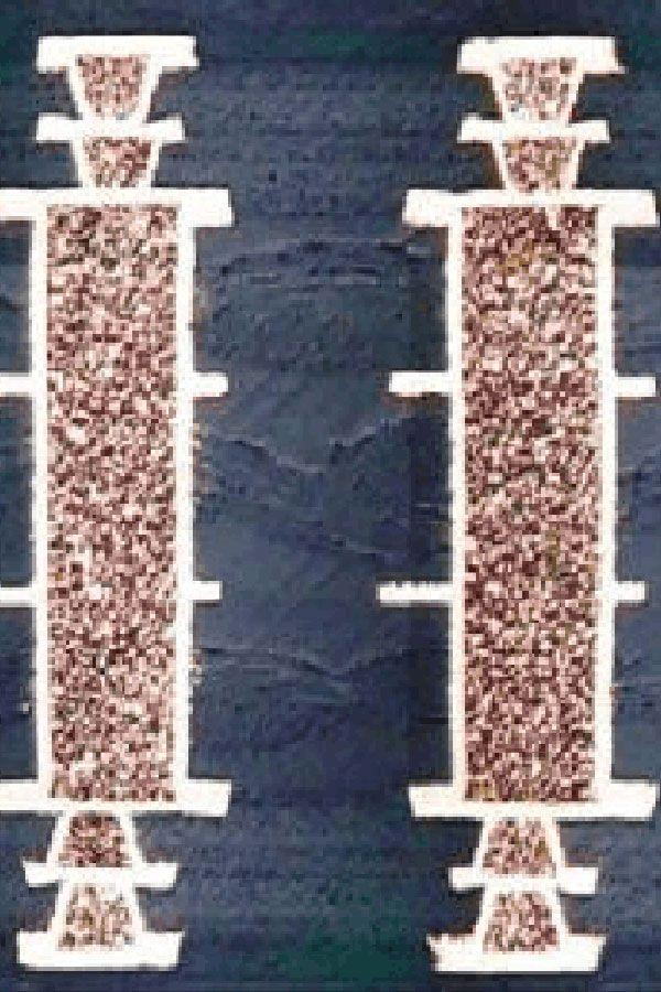
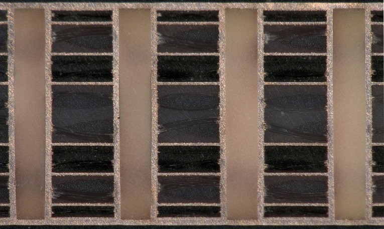
Vias filled with LPI/hole fill mask

Non-conductive via fill with epoxy hole fill

Planar copper surface above non-conductive via fill

Conductive via fill with silver paste
An overview of the HDI PCB Manufacturing can be found here: Microvia HDI PCB.
- Home
- Technology
- Epoxy Filled Vias
- PCB Technology
- PCB Material
- Epoxy Filled Vias
- Heavy copper circuit board
- HDI Micro vias PCB
- Controlled Impedance
- RF & Microwave PCB
- Rigid-Flex Circuit
- Bending And Folding
- Thermally Conductive PCB
- Flex PCB design guidelines
- Rigid flex PCB design guidelines
- HDI PCB design guidelines
- Heavy copper PCB design guidelines
- Flexible PCB design issues
- Flex-Rigid PCB design issues
- Turn-key PCB Assembly design issues
- PCB Trace Width Calculator
-
Phone:
-
Email:This email address is being protected from spambots. You need JavaScript enabled to view it.


