High Density Interconnect PCB Cost
Why Microvia PCB Technology?
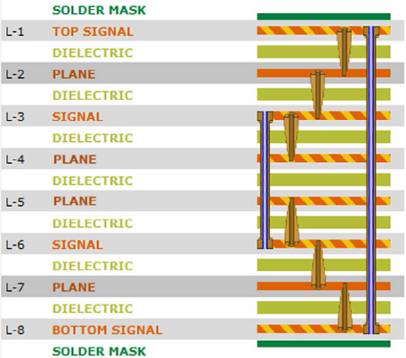
High Density Interconnect (HDI) circuit boards and microvia technology are inextricably linked. Microvias are tiny holes drilled with a laser. The subsequent metallisation creates an electrical connection between two adjacent copper layers in a multilayer.
In the miniaturization of printed circuit boards, microvias, placed directly in solder pads, play a decisive role as "microvia-in-pad". "Via-in-Pad" basically means that via holes are placed directly in the solder pads, saving valuable space. Since microvias are very small blind holes, they can also be integrated into very small solder pads. The solder deposit of the solder pad fills the minimal void. Optionally, buried vias are used, which are drilled mechanically and create space for components on the placement layers.
Thin copper foils with fine and ultra-fine conductor structures are another element of HDI technology. Together with microvias, the required wiring density for complex components can also be achieved on the printed circuit board.
Do you need HDI PCBs?
HDI is a necessity when the component pitch requires it, or the board size demands it. When properly designed, HDI PCBs are smaller, thinner, and weigh less (board downsizing trend). HDI has a myriad of constructions and variables that all affect density. To understand how blind vias, skip vias, staggered vias, stacked vias, and buried vias contribute to density, you must do a “routing test” and play with all these different stack-ups and constructions. By measuring the metrics (inches/square inch and pins/square inch), you can create a table that relates these density measures to the corresponding construction.
HDI PCB design techniques are used when considering the need to mount extreme component density on a limited board size. The component density determines the number of connections per square inch of the board. If the connections of all the parts and test points divided by the size of the board are less than 120 — 130 pins per square inch, there is no need to be using HDI, unless the use of specific dense BGA requires HDI to facilitate all connections. HDI technology has revolutionized the electronics industry and is used in most electronic gadgets you know. The demand for Printed Circuit Board using HDI technology looks promising for many various industries.
Are HDI PCB Boards Economical?
More than simply layers and laminations
Yes, multiple laminations cost more than a single lamination, but that’s merely one factor to consider in a thorough cost-benefi tanalysis when developing a stackup. First, let’s distinguish between prototype fabrication and production runs.
You have to hammer home to designers that they just can’t keep adding layers, making everything smaller, and fi gure the fab willjust have to deal with it. “Think strategically. Concentrate on yield from the beginning.” If you focus on the lowestinstalled cost, at some level of circuit complexity, you will have to carefully assess the HDI PCB cost versus not using HDI.
When a shop that specializes in prototype manufacture quotes a job for, say, 10 boards, and accepts the order, the shop is duty-bound to produce them, even though they may push the edge of process tolerances. A six-layer design with 3-mil drill-to-copperclearance might be produced readily, but holding registration in a 12-layer board with that spacing could be a very different story.Perhaps the manufacturer has to make 20 boards to yield 10 that are acceptable; perhaps the job has to be run twice. If there’s adelay in shipping the prototypes, what is the cost of that delay to the product development and introduction? What expense isincurred if temperature cycling causes eight of those 10 marginally good boards to short during use?
If the shop that gambled on building the 12-layer design had to make 20 boards to deliver the 10 ordered (and was able to deliverthem on time), the shop would have to absorb the 50% waste and bill the customer at the price quoted. However, if the customerneeds another batch, maybe with a few changes but the same basic architecture, the shop would then adjust the price tocompensate for the 50 percent yield. Still, for 10 revised prototypes that are urgently needed, the customer may have no choice but to pay the price increase or stall development. Too much has been invested in the design at this point to start fresh; moreover, the market window for the new product would close.If the revised prototypes survive testing, and the design is approved for production, the customer faces, at best, a 50% manufacturing yield: 10,000 boards would have to be fabricated to get half that many usable bare boards, and there would be someadditional loss in assembly. Inevitably, yield is the paramount cost consideration in PCBs, and somebody pays for it. The prototype fabricator who agrees to build the .rst order swallows the yield loss, hopefully at some profit. But the customer pays the freight from the next iteration through production.
Is HDI PCB Technology Necessary?
HDI technology is most suitable for boards with dense component placements, for example, BGAs on a very tight pitch. With conventional designs, it is possible to make such boards using through holes on a single-lamination. However, it would demand very small holes and very close hole-to-copper clearance. Not only is this design difficult to fabricate, the yield would be terribly low.
However, designing these boards with HDI technology makes it very easy for the designer. The BGA breakout requires 2.5 mil to 3 mil traces within the matrix, with connecting segments measuring 2 mils wide. The designer can use multiple sequential laminations to reduce the total number of layers, and apart from the BGA breakout traces, all traces can be 4-5 mils or even wider.
To make an economical HDI board, it pays to consult the manufacturing partner and seek their advice.
Type of via influences the HDI board cost
The via quality and plating of an HDI PCB has a direct relationship with the end product quality and HDI PCB cost. Mechanical drilling and laser drillings are the most commonly used via drilling formats. Mechanical drilling is the conventional drilling technique, which is still used as an efficient drilling method for through-hole vias and blind vias since it is economical.
If mechanical drills are used for drilling in HDI PCBs, high-speed spindles are combined with different kinds of depth sensors. The precise production of blind vias requires special techniques like drill depth control to ensure repeatable blind via formation.
The capital cost for mechanical drills is low compared to laser drilling. But it is not the same in case of operational cost. Also, a broken drill hole costs extra as it requires extra metallization and additional operating charge as well. So, for critical drilling and large-scale production laser drilling is preferred.
If we are comparing the cost of drilling one via, mechanical drilling is economic compared to laser drilling. But if we are considering the cost of 1000 vias with high precision, consistency of drill quality, and high-speed processing, laser drilling is economical. Choosing the right drilling technology is one of the crucial factors for optimizing the HDI PCB cost.
Laser Drill Technology
Drilling the smallest of micro-vias allows for more technology on the board's surface. Using a beam of light 20 microns (1 Mil) in diameter, this high influence beam can cut through metal and glass creating the tiny via hole. New products exist such as uniform glass materials that are a low loss laminate and low dielectric constant. These materials have higher heat resistance for lead free assembly and allow for the smaller holes to be used.
Lamination & Materials For HDI Boards
Advanced multilayer technology allows for designers to sequentially add additional pairs of layers to form a multilayer PCB. The use of a laser drill to produce holes in the internal layers allows for plating, imaging and etching prior to pressing. This added process is known as sequential build up. SBU fabrication uses solid filled vias allowing for better thermal management, a stronger inter connect and increasing the board's reliability.
Resin coated copper was developed specifically to aide with poor hole quality, longer drill times and to allow for thinner PCBs. RCC has an ultra-low profile and ultra-thin copper foil that is anchored with minuscule nodules to the surface. This material is chemically treated and primed for the thinnest and finest line and spacing technology.
The application of dry resist to the laminate still uses heated roll method to apply the resist to core material. This older technology process, it is now recommended to preheat the material to a desired temperature prior to the lamination process for HDI printed circuit boards. The preheating of the material allows for better a steady application of the dry resist to the surface of the laminate, pulling less heat away from the hot rolls and allowing for consistent stable exit temperatures of the laminated product. Consistent entrance and exit temperatures lead to less air entrapment beneath the film; this is critical to the reproduction of fine lines and spacing.
LDI & Contact Imagery
Imaging finer lines than ever before and using semiconductor Class 100 Clean rooms to process these HDI parts is costly but necessary. Finer lines, spacing and annular ring requires much tighter controls. With use of finer lines, touch up rework or repair becomes an impossible task. Photo tool quality, laminate prep and imaging parameters are necessary for successful process. Using a clean room atmosphere decreases defects. Dry film resist is still the number one process for all technology boards.
Contact imaging is still widely used due to cost of laser direct imaging; however, LDI is a far better option for such fine lines and spacing. Currently most factories still use contact imaging in a SC100 room. As the demand expands, so does the need for laser drilling and laser direct imaging.
The importance of communicating with PCB manufacturers
Let us interject a disclaimer: Though our company has extensive experience with the three materials, that experience isn’t quantified and therefore must be considered subjective. There’s no bias toward one rather than the others, except for HDI from manufacturing experience. We’ll build whatever a customer wants if it can be constructed. The point to bear in mind is simply this: If a board is challenging to build in limited, prototype quantities, it will be no less challenging to manufacture in production runs. To repeat, yield drives profit.
Our company, Hemeixin, has found that achieving clean laser-drilled holes in the Nelco material and in FR408HR requires more effort compared to creating them in Megtron 6. The resin in the Nelco fabric burns off at a much different rate than the glass fibers and too much energy is required to consume all the fibers in the hole without compromising the surrounding dielectric and the landing pad itself. FR408HR is less prone to have glass fibers protrude from hole walls than is N4000-13 SI but is less predictable in that respect. Glass bundles extend in perhaps only 5% of the holes but such inconsistency itself complicates processing. The flat glass fabric of Megtron 6 can be ablated cleanly by contrast to the other two materials, in our experience.
Nelco is continually investigating resin formulations, glass, and fabric constructions that would improve the manufacture of HDI architectures. The firm recently introduced a new material, N4800-20 SI, which it recommends in place of N4000-13 SI for HDI PCB manufacture. Our company is evaluating that material and anticipates better results.
To summarise, in order to get the optimal HDI PCB cost, one has to consider several factors such as yield, material type, via drilling methods, and imaging. The advantage of HDI is higher yield due to better control of drill to copper and use of traces above 3 mils. HDI also results in a lesser number of PCB layers.
The upshot of all this is that you should consult your board manufacturer at the outset of design to identify materials that would provide the optimum balance of price, manufacturability, and performance based on your construction. We’ll dedicate this column as the first installment regarding materials and manufacturability. The next one will regard materials with the highest electrical performance for digital high-speed circuits, and for RF and microwave applications.


