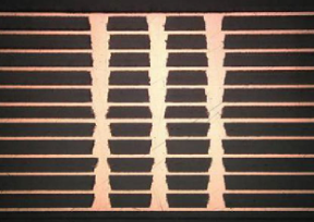
What is microvia
As it's name suggests, a microvia is just a very small version of a typical via, but the structure is a bit different. Microvias have conical frustum shape; the via slopes inwards as it makes a layer transition and terminates at a pad in the next layer. Ideally, microvias will only span a single layer for maximum reliability. Designers can use stacked microvias to form connections across multiple layers, where blind and buried microvias are built up into a stack to reach across multiple layers.
Microvias are the fastest growing new technology for printed circuits. This talk will highlight the procedures, standards and conditions that designers needs to consider to introduce microvias to their printed circuit board designs. The basis for these procedures is the IPC-2226, IPC-4104 and IPC-6016 HDI standards.
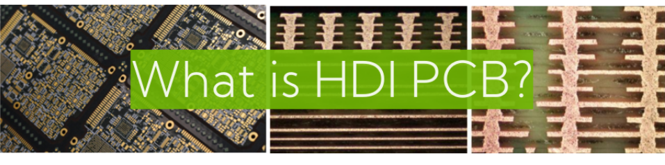
HDI PCB structures
The IPC-2226 defines the structures of HDI PCB by type, there are three types and we can observe in the images highlighted.
Type I structures
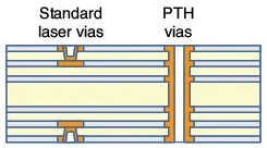
Those that contain a single layer of microvia on one or both sides of the core. It uses both microvias and through holes for interconnection. It is important to keep the ratio 0.8: 1 for the microvia. This structure uses ONLY blind holes NO passage to buried holes.
Type II structures
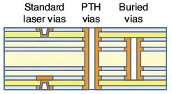
Are similar to type 1 in that they contain only a single layer of microvia on one or both sides of the core. It uses both microvia and through holes for interconnection, but unlike type 1 these structures also use buried holes.
Type III structures
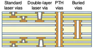
Are the most complex and demanding for factories, they contain AT LEAST two layers of microvia on one or both sides of the core. As for type 2, it also uses through holes in addition to blind and buried vias.
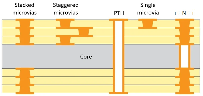
Any layer HDI PCB Stackups
More generally, this structure is known as an any layer HDI PCB stackup, where the outer sections consist of i sequentially laminated layers connected with microvias. The inner portion of the layer stack is connected to the outer sections at the top and bottom ends with a buried via, and the buried via portion (called a core via) also connects to the other inner layers. You could conceivably use any number of sequentially laminated layers on the outside of the stackup as long as it can be produced by your fabrication house. For example, 3+N+3 and 4+N+4 layer stacks are also common options provided by HDI PCB fabrication houses.
Also, there is technically no limit to N in theory, although practically this will be limited depending on the outer layer thickness and the total layer count. The reliability issues (to be discussed more below) found in microvia stacks is not present on this inner layer as a mechanically drilled through-hole is used to connect the inner layers before lamination with the outer layers. This forms a buried via once the entire stackup is built up. Once the stackup is built up, through-holes can also be placed in the finished layer stack going between all layers using standard drilling and plating processes.
Featuring a combination of laser technology, filled plating technology, etc. Capable of ultrafine processing, these PCBs permit flexible connections across all layers. Because these PCBs enable a high degree of design flexibility and integration, they are ideally suited to increasing needs for smaller and thinner high-performance devices such as smartphones.
Microvia PCB Fabrication
Exactly how small are microvias? If you ask most designers, they might tell you that they would consider a microvia to be a via with a diameter less than about 150 µm (6 mils). Depending on the size of the vias, they can be mechanically drilled and plated (followed by stacking and pressing each layer), or they can be formed with a high-power laser. The latter process is constantly being improved and is preferred in high volume PCB manufacturing thanks to its high throughput. New advances in laser drilling techniques are pushing microvia sizes down to as small as 15 µm.
After drilling and cleaning, the via hole is plated, either with a sputtering process, electrolytic deposition, or electroless copper plating process. The goal in the plating process is to prevent the formation of voids, dimples, bumps, or any other structural defect in the filled via. Voids are also a reliability concern as stress can concentrate around the edge of the void where copper is thinner if stress is applied to the via structure.
During fabrication, laser-drilled microvias have a lower potential for manufacturing defects than normal vias. Mechanically-drilled microvias can have defects due to drill vibration as the drill wears out, and mechanical microvia drilling is only useful down to 6 to 8 mil diameters, depending on the fabricator's tooling investments.
Types of Microvias
There are a few different types of microvias. All microvias have two common characteristics:
Low aspect ratio: Contrary to through-hole vias in typical PCBs, microvias have small aspect ratio. The aspect ratio of these vias is preferably 0.8:1. Larger aspect ratios of 1:1, or even as high as 2:1, can be fabricated, but they bring reliability concerns. Because of this, they typically only span between a single layer. Note that a microvia aspect ratio that is greater than 1 does not meet the IPC definition of a microvia.
Susceptible to fracture at the neck: High aspect ratio through-hole vias (~10:1) tend to be most susceptible to fracture near the middle of the via barrel. Due to the plating method used in microvias, copper curves inward to the barrel region and stress tends to concentrate there. As a result, microvias are most susceptible to fracture in the neck region under repeated thermal cycling, strong vibration, or mechanical shock.
Aside from these qualities, the differences between microvias are simply their typical diameter and where they appear in a circuit board. Microvia-in-pad configuration is common with fine-pitch BGA components, where the small distance between solder balls will not allow a dog bone fanout. Microvias on the surface layer can also be placed in a pad, filled with a conductive epoxy or electrodeposited copper, and plated over with copper (this is the microvia analogue of via-in-pad plated over, or VIPPO, for standard via sizes). The in-pad configuration has advantages in that the pad is now solderable, but the internal fill and the copper wrap plating on the via are now the main reliability concerns.
This illustration should the general uses and types of microvias that can be placed in an HDI PCB. Note that you can have a traditional buried via structure or through-hole structures in the same layer as microvias (see the PCB layout image above).
With these points in mind, here are the different types of microvias:
Blind Microvias
Blind microvias start in the surface layer and terminate 1 layer below the surface, although they could terminate or 2 layers below the surface layer if the aspect ratio is kept low. If you need to span 2 layers, it's better to use stacked microvias (see below) or staggered microvias as these will be more reliable. Blind microvias could be filled or unfilled.
Buried Microvias
Buried microvias have basically the same structure as blind vias and span between two interior layers and do not reach either circuit board surface. Just like blind microvias, it's best the aspect ratio stays low and they span a single layer to ensure reliability and ease of fabrication. These vias are filled with copper, either using a plating process with pure copper or with a epoxy + copper resin to ensure a strong connection across the head of the microvia. It's important that the process being used for plating results in void-free structures to ensure maximum reliability.
Stacked and Staggered Microvias
You may be a bit hesitant to try incorporating lots of buried and blind vias into your designs, but the layer-by-layer process for forming low aspect ratio microvias makes them useful in stacked applications. Stacked microvias are simply stacks of buried vias, or a blind microvia stacked on top of buried microvias. This is the standard way to span between multiple layers in an HDI PCB. The internal buried microvias in the stack need to be filled with conductive paste and plated over to ensure strong contact as the next via in the stack is deposited and plated. The alternative to stacked microvias is staggered microvias, where microvias on successive layers are offset from each other.
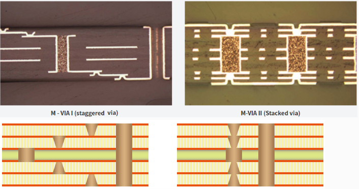
The design decision that needs to be made with stacked and staggered microvias, as well as individual blind/buried microvias, is the aspect ratio to be enforced in the design. Stacking is also important due to potential failure at the interface between vias in a stack.
Microvias Filled or Unfilled?
Microvias can be either filled or unfilled with copper. For buried microvias, it's important to fill the via hole with copper, especially if there will be any stacking. If any voids are left over in the interior of the via plating, then the via will experience high stress concentration along the via wall, which could lead to premature fracture during reflow or during operation. Blind microvias can be left unfilled, and this was typical in the early days of microvia fabrication and implementation. If blind microvias will be used in-pad, then they should be filled with a standard process.
The manufacturer will use pure copper or an epoxy +copper resin for plating. The typical process normally begins with conformal plating, followed by pulsed plating to fill in the body of the microvia with solid copper and eliminate voids. Plating processes that do not use some additive in the filler material typically results in void formation inside the body of the plating volume. Even if the microvia body is totally filled with copper, the copper may concentrate along the walls and the top surface of the if additives are not used during plating. Conformal plating also contributes to an uneven deposition of copper along the via body, leading to voiding.
HDI PCB Capabilities
Refer to the chart below for Hemeixin's HDI / Laser Drilled Microvia (μVia) Capabilities
| Smallest (as ablated) Laser Microvia | 0.003" |
| Largest (as ablated) Laser Via | 0.010" |
| Microvia Aspect Ratio (Depth to Diameter) |
0.80:1 Standar / 1:1 Advanced |
| Capture Pad Size | μVia +0.008" Std. / μVia +0.006" Adv. |
| Landing Pad Size | μVia +0.008" Std. / μVia +0.006" Adv. |
| Stacked Microvia | Yes |
| Type I Capabilities | Yes |
| Type II Capabilities | Yes |
| Type III Capabilities | Design Dependent |
| Copper Filled Microvias | Yes |
High-density interconnects are categorized by six design types in IPC-2226. They are grouped by stackup characteristics in the following categories: Type I, Type II, Type III, Type IV, Type V, and Type VI
- TYPE I 1 [C] 0 or 1 [C] 1, with through-vias from surface to surface.
- TYPE II 1 [C] 0 or 1 [C] 1, with buried vias in the core and may have through-vias connecting the outer layers from surface to surface.
- TYPE III 2 [C] 0, two or more HDI layers added to through-vias in the core or from surface to surface.
- TYPE IV 1[P] 0 where P is a passive substrate with no electrical connecting functions.
- TYPE V Coreless constructions using layer pairs.
- TYPE VI Alternate constructions of coreless construction using layer pairs.
Conclusion
Microvias and stacked microvias can be found in High Density Interconnect circuit boards, also known as HDI PCBs, to enable complex interconnections in advanced designs.
Microvias, stacked microvias, and via-in-pad features allow miniaturization for higher functionality in less space and can accommodate large pin-count chips such as the ones used in cell phones and tablets. Microvias help reduce layer count in printed circuit board designs while enabling higher routing density and eliminating the need for through vias.
HDI PCB design is a critical process that requires careful consideration of various factors. By following the HDI PCB design guidelines and considering the key factors mentioned in this blog, designers can create innovative and reliable HDI designs and enable the realization of innovative and cutting-edge products. Hemeixin, a leading PCB manufacturer in China, has been engaged in PCB design for nearly 15 years. We own all expertise and tools required to complete powerful HDI PCB design, our team of experts has served customers from various industries ranging from medical, and consumer electronics, to automotive, and IoT.


