What are Microvias Flexible PCB and rigid flex PCB
Flexible printed circuit boards (FPCs) offer the highest level of 3D miniaturization. Very low bending radii in combination with ultra fine lines enable our customers to build increasingly smaller and highly integrated devices.
Hemeixin production facility have been in this field for many years and manufacture flexible circuits up to 16 layers!
We are working with polyimide foils as thin as 12.5 µm and adhesive bond plies starting at a thickness of 12.5 µm. State of the art equipment enables us to produce FPCs with high output, reliability and repeatability. Depending on the dielectric thickness, laser drilled blind via’s can be as small as 35 µm in diameter and filled with copper in the subsequent plating process to support the use of stacked via’s and via-in-pad structures.
High-end alignment tools make it possible to achieve very small annular rings and solder mask registration even on extremely complicated multilayer FPCs. As an option, also cover layer foils can be used.
High accuracy laser contour cutting & optimized the space utilization make it possible to achieve excellent 3D miniaturization for small wearable (medical) devices as well as high signal density COF (chip on flex).
Via holes in flexible circuit board designs
Devices are becoming smaller and thinner, requiring circuit boards that can fit into the equipment without adding any additional weight while being flexible enough to route around components. Flexible printed circuit boards offer high-density electrical connections while also reducing space.
Along the circuit board, flexible films and conductive materials are placed in layers. The number of layers used is dependent on the complexity of the design. To connect the electrical signal between the varying layers, a via hole is placed on the PCB.
Types Of Flex PCB Vias
Through-hole/Thru-hole: The term via and through-hole are sometimes used interchangeably. However, a through-hole is a via that goes all the way through the layers of the printed circuit board to the other side.
Buried Via: A buried via is an internal via. It does not meet to an external layer of the surface of the board and instead connects internal layers. Example: via that connects only layers 2 and 3 in a 4-layer design.
Blind Via: A blind via only goes partway through the board as it starts at the external layer. Example: via connects only Layers 2 and 3 in a 4-layer design.
Microvias: A microvia is a via with a diameter of less than 0.006 inches. Unlike the other vias that are made with a mechanical drill, microvias are drilled using a laser.
Microvias Flexible PCB
Microvias are holes through one or more layers of a flexible circuit board made of alternating insulating and conducting layers of material. These materials are often copper sheet (1/2 oz typically) and an epoxy/fiberglass blend in thin sheets (.001-.002” thick). The laser drilling tool will create a via from the top layer down to a copper catch pad below which will be plated to form an electrical connection between conducting layers.
High Density Interconnect (HDI) flex circuits offer designers the same benefits of flex circuits—smaller, more reliable products—except at a higher level. In addition to the design benefits of HDIs and microvias listed below, HDI circuits give you more design, layout and construction options helping you finish your design in less time.
Lower cost and smaller size - increased circuit density can eliminate extra layers and save up to 40% compared to non-HDI designs.
Use advanced component packaging - high-I/O and fine-pitch feature capabilities possible with HDI.
More design options and flexibility - blind and buried microvias allow for conductor routing on the internal layers under vias, creating more usable design space per layer.
Improved electrical performance and signal integrity - microvias in high-speed circuits improve electrical performance by allowing shorter circuit paths, stub reduction and lower cross talk and noise.
Improved thermal performance and reliability - microvias lower the z-axis thermal stresses between adjacent layers.
Improved cost effectiveness - Hemeixin's 18" x 24" (45.7 cm x 61 cm) panel size maximizes circuit density to increase the efficiency of your assembly process
HDI Flex PCB Design Options
Flex PCB and rigid-flex PCB design and layout are interrelated; the major difference between flex and rigid-flex is an interconnect spanning into the rigid ends of the board. Much like a standard rigid PCB, the flex PCB design process starts with designing a stackup, placing components, planning and routing paths for traces, and finally cleaning up the layout to prepare for manufacturing. Some additional steps are required to ensure the flex section has the required mechanical properties, such as adding stiffener, selecting a coverlay or photoimageable solder mask material, or setting a static bend in the design.
- Single-layer, double-layer, multilayer and rigid-flex circuits with high layer counts to meet your interconnection needs
- Fine lines, circuit forming and selective bonding add to space and weight savings
- Stiffeners, pins, connectors and full turnkey electronics packaging for efficient integration into your application
- Inductive communication coils can be integrated with flex circuits to provide critical communication assemblies
- Minimum microvia size: 75 micron, 50 micron finished
- Minimum microvia pad size: via diameter +150 microns
- Minimum line and spacing: 50 micron Microvia blind plating aspect ratio (depth to diameter): 1:1
- Minimum core dielectric thickness: 25 micron
- Minimum copper thickness: 9 micron
- Blind & buried via construction: sequential build technology
- Via fill: copper via fill available
Hemeixin’s Rigid Flex PCB Capabilities
Hemeixin’s Rigid Flex assemblies offer the advantages of both flexible cables and conventional PCBs. The rigid portions allow you to have surface mount SMT components down to 0201 on both top and bottom surfaces within the same region. They also can be designed to utilize conventional through-hole connectors and components, and our ability to add heaters and sensors to flex and rigid flex circuits helps create solutions that reduce assembly errors and improve time-to-market. Our unsurpassed capabilities allow us to integrate any combination of our high-quality flex circuits, heaters, sensors, and other components into a single solution.
Special considerations for rigid-flex PCB
- Rigid-flex is the ideal solution for applications with multiple rigid PCBs having SMT components on both sides and requiring interconnects between the rigid PCBs.
- Before designing a rigid-flex circuit, make certain that it is truly what you need. If the circuit only has a few layers, stiffeners are a less expensive alternative to rigid-flex.
- It is most cost effective to build a rigid-flex with an even number of layers. All rigid portions of the circuit should have the same number and stack-up of layers.
- Observe aspect ratio (hole depth/hole diameter) limits.
- Hemeixin builds circuits up to 20 layers, but costs increase significantly above 10 layers.
- Expect a trim tolerance similar to that of a steel rule die from hole-to-border and border-to-border.
- Hole positional tolerance within a cluster of holes is generally +/-.002”. Add .001” per inch for tolerances between cluster datums, especially those in different rigid areas.
- Minimum inside corner radius of 0.031” (0.79mm) is standard, but smaller radii are possible.
- Unbonded layers can increase flexibility in multilayer flex circuits, but this option is more expensive. Specify unbonded layers only in areas of the circuit that will bend.
- Hemeixin can provide an epoxy fillet on stiffener edges that will bend or flex.
- For rigid-flex circuits, it is less expensive to have plated through-holes in the rigid portions only
Via in pad technology in flex pcb and rigid flex pcb
Many of today’s rigid-flex circuit designs utilize the same high-density components found in rigid PCB designs. This requires the use of blind and or buried vias to allow the signal lines to be routed out from within the high-density components or the high-density areas of the design. The most common component that we see driving this today is the 0.4mm pitch BGA package.
Blind vias allow the signals to be dropped down to the next layer from within the BGA SMT pad and then routed out from there. In high pin count devices, additional blind and or buried vias may be required. Differences exist in how blind and buried vias can be implemented in a rigid–flex design due to the materials and manufacturing processes required.
Blind & Buried Via Material Stack Ups
While there are potential constraints with blind and buried vias that need to be factored into a rigid–flex design, there are a wide variety of configurations that can be applied to resolve high density routing requirments.
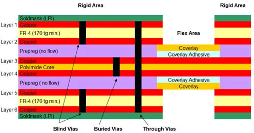
The 1st example is a 6-layer construction with 2 flex layers. This utilizes 2 blind vias from the external layers down to the next internal layers and 1 internal buried vias between the flex core layer pair. This construction does not require any additional or sequential lamination processes
.
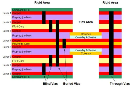
The 2nd example is a more complex 8-layer design with 2 flex layers. A sequential lamination cycle is required. Layers 2-7 are laminated together and blind vias from Layers 2 to 3 and from layers 7 to 6 as well as the buried via from layers 2 to 7 are drilled and plated. Layers 1 & 2 are then laminated using a foil outer construction method and blind vias from layers 1-2 and from layers 8-7 and the through vias from layers 1-8 are drilled and plated
.
A common item with both above configurations is that the finished thickness may be limited by the blind via requirement to maintain a max 1:1 aspect ratio. If a specific thicker rigid area dimension is needed it may be achieved by adding additional layers of FR4 and pre-preg.
Controlled impedance requirements may also impact the design due to the dielectric spacing between layers required to achieve the specific impedance values.
Via In Pad & Via Fill
Many designs that utilize blind and buried vias also require the blind and/or through vias to be located within the SMT pads on the external layers. This then requires the vias to be filled and capped with copper to ensure a flat co-planer SMT pad and to prevent solder from being drawn into an open via which could potentially starve the solder joint of solder. This process is the same as the rigid PCB process and can be applied to all rigid-flex designs.
Can via-in-pad be used on a flexible PCB or rigid-flex circuit with SMT parts?
SMT is successfully implemented on flex and rigid-flex every day. Standard through-hole constructions are the most cost-effective, but in some cases there is no room for through-holes and their larger pad diameters. Via-in-pad is a design strategy that may be required with very tight pitch BGA components and other SMT devices on flex and rigid-flex. The advantage of using a microvia is the hole size is quite small, and the associated pad is small as well. This provides more real estate for routing signals, especially out of BGA patterns. The rules-of-thumb and considerations are different, however, depending on whether the part is purely flex or rigid-flex.
For a pure flex, where all the material is flexible, consider a couple of things. Typically, via depths are much shallower than for a rigid or rigid-flex part. This means less solder may be consumed in the PTH. In some cases, the hole must be plugged, however.
Because flex is thin and flexible, standard via filling does not work well. Flex circuits tend to have more surface topography, making it hard to keep fill material out of low-lying areas in the panel. More important, planarizing can damage thin flex materials. The sanding operation can stretch and rip the flex apart. Nonconductive via fill is not really an option for pure flex.
If the vias cannot be filled, then what can we do? Microvias are the most common option. For a two-layer flex, vias can be created either from layer 1-2 or 2-1. This leaves the pad on the one side undisturbed. If vias are created from the side opposite any SMT pad, there is no need for plating the vias full.
For three or more layers of flex, there is a dimple where the via is placed. Depending on the material stackup, the dimple may be so shallow that copper filling is not needed. If it is, however, this can be easily achieved with copper plating.
Generally, microvias in flex are best when lasered into all polyimide flex substrates that do not use adhesive to bond the foil to the substrate. Polyimide lasers cleanly, with a smooth sidewall. If there is adhesive in the via hole, some undercut of the adhesive is likely to be seen in the hole because the laser and subsequent hole prep operations tend to attack the adhesive more than the polyimide. This is okay, so long as the undercut does not become so severe as to create plating folds or voids.
For rigid-flex, fabricators generally follow the same strategies as for a rigid PCB. We do a standard via-in-pad through-hole, fill it with epoxy, and then plate over it. This assumes the design has room for a through via and associated pad. As a rule-of-thumb, the pad needs to be about 14 to 16 mils larger than the drill size. If, then, we are drilling at 10 mils, the pad should be about 26 mils in diameter.
If there is no room for this, a combination of buried vias and microvias may be used. The microvias permit small SMT pads externally and larger pads internally, where more room may exist. Depending on device pitch and pin count, more than one layer of microvias may be needed to route everything out.
The caveat for rigid-flex: buried vias need to be filled. As a result, external layers of the buried via must be rigid material to avoid damage that would occur if the external layer were flex. This may require an extra internal rigid layer, either a pad or plane layer.
A quick comment on epoxy fill. Today, virtually all epoxy fill material is nonconductive. As vias shrunk, it became too difficult to drive conductive epoxy into the holes. Also, the fabricator likely has an aspect ratio limit on the via fill operation. Most are not able to fill holes greater than 10:1 aspect ratio. Also, somewhere near 8 to 10 mil drilled holes are the minimum size, where they can reliably drive the epoxy into the holes and fill them.
Most fabricators recommend microvias of at least 0.005" in diameter, with pads between 0.010" and 0.012" diameter. While the microvia depth to diameter aspect ratio may be quite low, it may not be advised to create a smaller diameter microvia. Historical data indicate via reliability begins to be reduced below 5 mils and drops significantly below 4 mils. The real estate gained may not be worth the reduction in system reliability.
In any of these constructions, avoid stacking microvias, especially more than two high. Recent industry experience seems to indicate stacked microvias in any board type may be prone to failure after a high number of thermal cycles. Staggering vias seems to increase the cycle count substantially. IPC members are investigating this phenomenon to better understand the failure mechanism and determine a way to resolve the condition. In the meantime, be safe and stagger if possible.
Staggering has another advantage: internal microvias do not require copper filling to permit the next via to be placed directly on the previous one. Staggering does put extra burden on the designer but will pay benefits in the long run.
SMT is common. The number of different via structures and laminations have a significant impact on unit cost. Sometimes, your supplier can modify structures to minimize the number of laminations or piggyback some plating operations to eliminate duplicate operations. This can have a big impact on costs.
In conclusion, add vias directly in SMT pads to provide the necessary room to route the rest of the circuit without impacting the ability to solder SMT components.


